134
7598H–AVR–07/09
ATtiny25/45/85
Flash corruption can easily be avoided by following these design recommendations (one is
sufficient):
1. Keep the AVR RESET active (low) during periods of insufficient power supply voltage.
This can be done by enabling the internal Brown-out Detector (BOD) if the operating
voltage matches the detection level. If not, an external low V
CC
reset protection circuit
can be used. If a reset occurs while a write operation is in progress, the write operation
will be completed provided that the power supply voltage is sufficient.
2. Keep the AVR core in Power-down sleep mode during periods of low V
CC
. This will pre-
vent the CPU from attempting to decode and execute instructions, effectively protecting
the SPMCSR Register and thus the Flash from unintentional writes.
20.4.5 Programming Time for Flash when Using SPM
The calibrated RC Oscillator is used to time Flash accesses. Table 20-1 shows the typical pro-
gramming time for Flash accesses from the CPU.
21. Memory Programming
This section describes the different methods for Programming the ATtiny25/45/85 memories.
21.1 Program And Data Memory Lock Bits
The ATtiny25/45/85 provides two Lock bits which can be left unprogrammed (“1”) or can be pro-
grammed (“0”) to obtain the additional security listed in Table 21-2. The Lock bits can only be
erased to “1” with the Chip Erase command.
Program memory can be read out via the debugWIRE interface when the DWEN fuse is pro-
grammed, even if the Lock Bits are set. Thus, when Lock Bit security is required, should always
debugWIRE be disabled by clearing the DWEN fuse.
Note: 1. “1” means unprogrammed, “0” means programmed
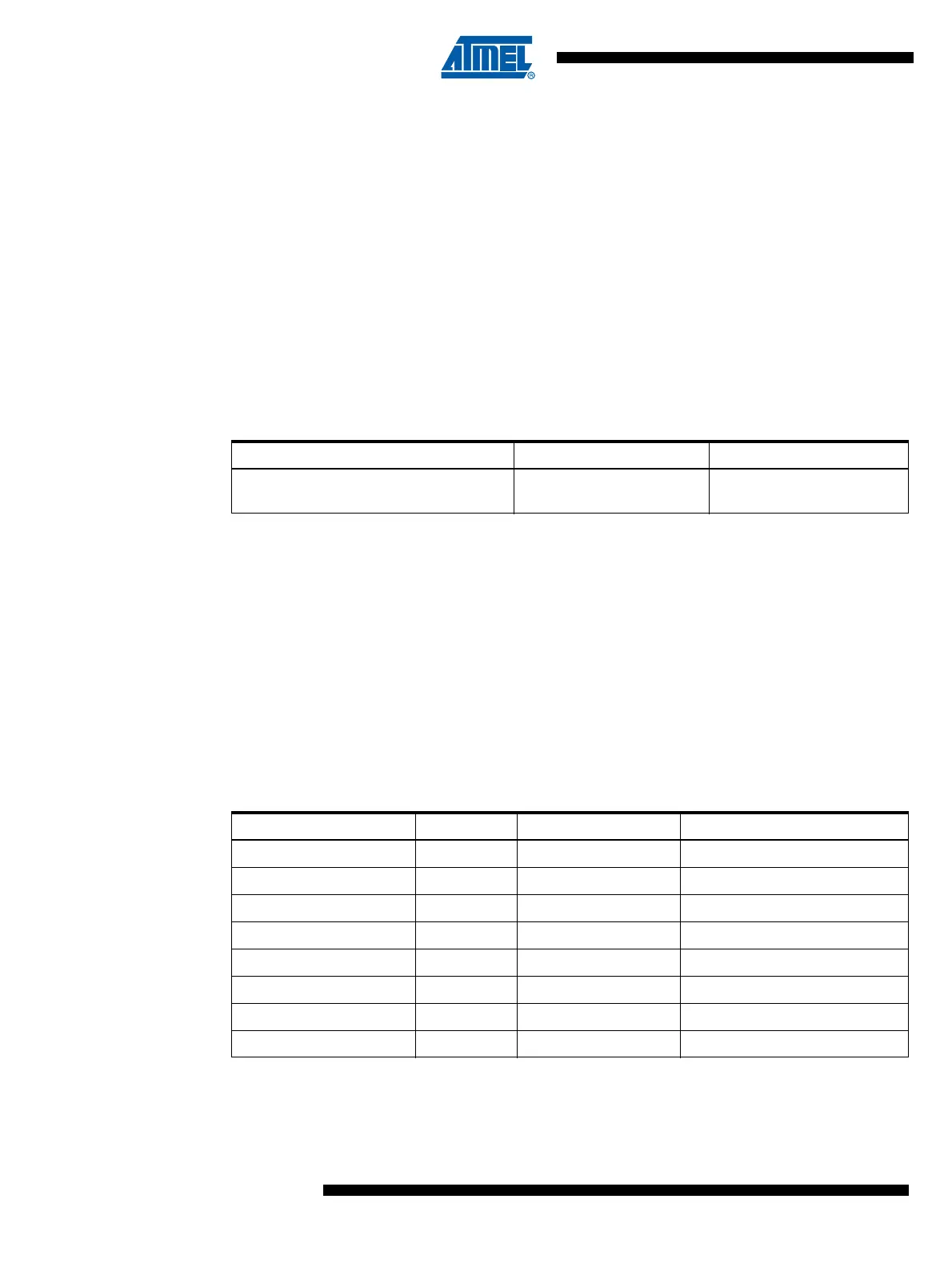
Table 20-1. SPM Programming Time
Symbol Min Programming Time Max Programming Time
Flash write (Page Erase, Page Write, and
write Lock bits by SPM)
3.7 ms 4.5 ms
Table 21-1. Lock Bit Byte
()
Lock Bit Byte Bit No Description Default Value
7 – 1 (unprogrammed)
6 – 1 (unprogrammed)
5 – 1 (unprogrammed)
4 – 1 (unprogrammed)
3 – 1 (unprogrammed)
2 – 1 (unprogrammed)
LB2 1 Lock bit 1 (unprogrammed)
LB1 0 Lock bit 1 (unprogrammed)