47
7598H–AVR–07/09
ATtiny25/45/85
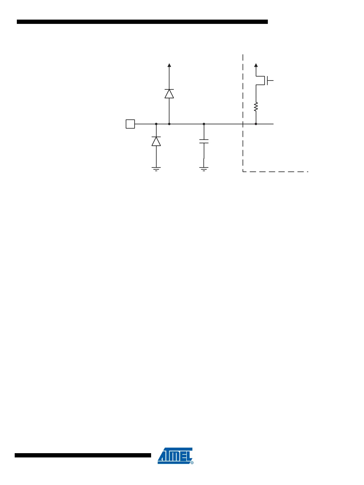
Figure 10-1. I/O Pin Equivalent Schematic
All registers and bit references in this section are written in general form. A lower case “x” repre-
sents the numbering letter for the port, and a lower case “n” represents the bit number. However,
when using the register or bit defines in a program, the precise form must be used. For example,
PORTB3 for bit no. 3 in Port B, here documented generally as PORTxn. The physical I/O Regis-
ters and bit locations are listed in “Register Description for I/O-Ports” on page 58.
Three I/O memory address locations are allocated for each port, one each for the Data Register
– PORTx, Data Direction Register – DDRx, and the Port Input Pins – PINx. The Port Input Pins
I/O location is read only, while the Data Register and the Data Direction Register are read/write.
However, writing a logic one to a bit in the PINx Register, will result in a toggle in the correspond-
ing bit in the Data Register. In addition, the Pull-up Disable – PUD bit in MCUCR disables the
pull-up function for all pins in all ports when set.
Using the I/O port as General Digital I/O is described in “Ports as General Digital I/O” on page
47. Most port pins are multiplexed with alternate functions for the peripheral features on the
device. How each alternate function interferes with the port pin is described in “Alternate Port
Functions” on page 52. Refer to the individual module sections for a full description of the alter-
nate functions.
Note that enabling the alternate function of some of the port pins does not affect the use of the
other pins in the port as general digital I/O.
10.2 Ports as General Digital I/O
The ports are bi-directional I/O ports with optional internal pull-ups. Figure 10-2 shows a func-
tional description of one I/O-port pin, here generically called Pxn.
C
pin
Logic
R
pu
See Figure
"General Digital I/O" for
Details
Pxn