182
7598H–AVR–07/09
ATtiny25/45/85
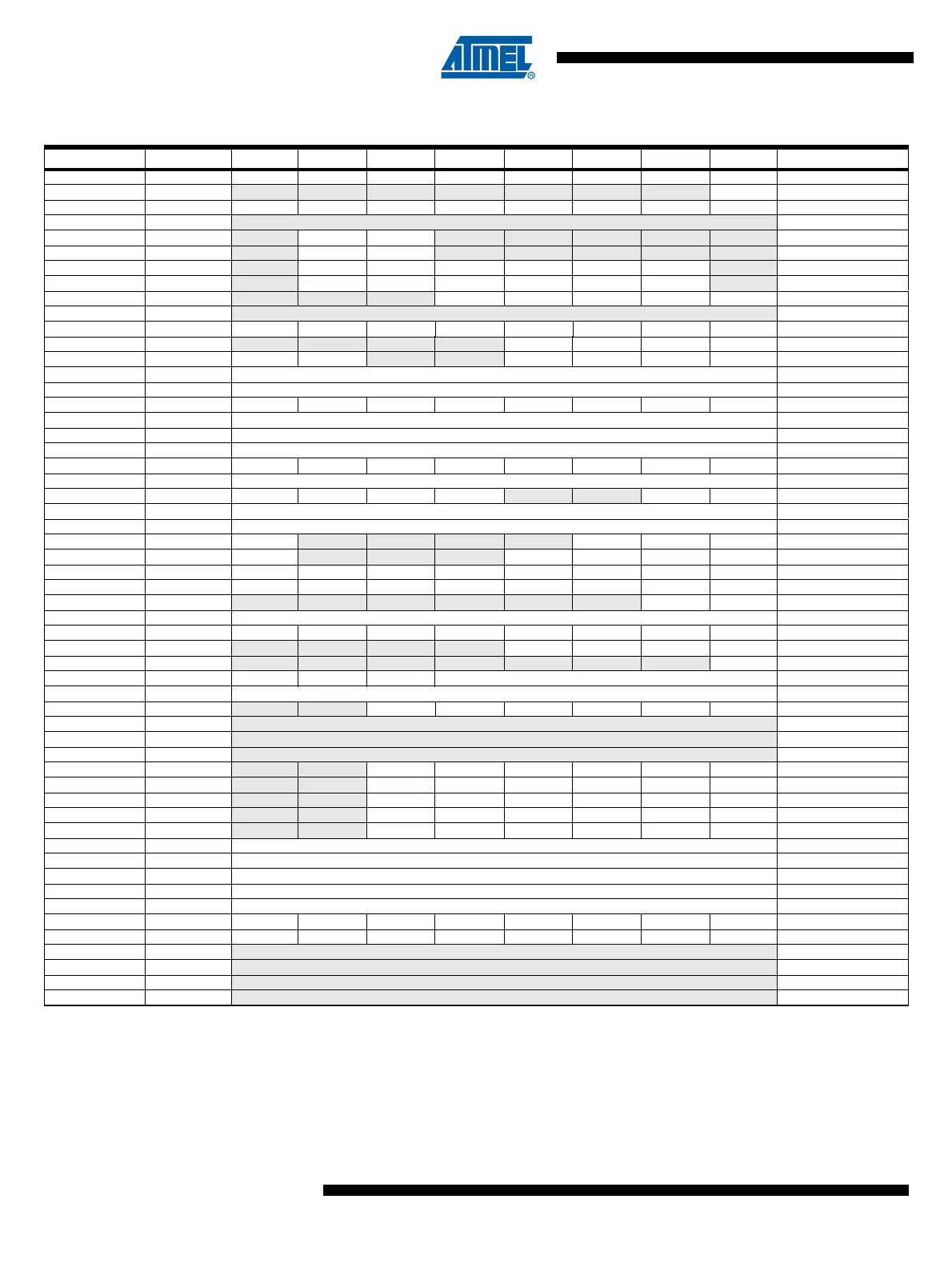
24. Register Summary
Address Name Bit 7 Bit 6 Bit 5 Bit 4 Bit 3 Bit 2 Bit 1 Bit 0 Page
0x3F SREG I T H S V N Z C page 7
0x3E SPH – – – – – – – SP8 page 10
0x3D SPL SP7 SP6 SP5 SP4 SP3 SP2 SP1 SP0 page 10
0x3C Reserved –
0x3B GIMSK – INT0 PCIE – – – – – page 59
0x3A GIFR – INTF0 PCIF – – – – – page 60
0x39 TIMSK – OCIE1A OCIE1B OCIE0A OCIE0B TOIE1 TOIE0 – page 77
0x38 TIFR – OCF1A OCF1B OCF0A OCF0B TOV1 TOV0 – page 77
0x37 SPMCSR – – – CTPB RFLB PGWRT PGERS SPMEN page 132
0x36 Reserved –
0x35 MCUCR BODS PUD SE SM1 SM0 BODSE ISC01 ISC00 page 31, page 54, page 59
0x34 MCUSR – – – – WDRF BORF EXTRF PORF page 40
0x33 TCCR0B FOC0A FOC0B
– – WGM02 CS02 CS01 CS00 page 75
0x32 TCNT0 Timer/Counter0 page 76
0x31 OSCCAL Oscillator Calibration Register page 26
0x30 TCCR1 CTC1 PWM1A COM1A1 COM1A0 CS13 CS12 CS11 CS10 page 84
0x2F TCNT1 Timer/Counter1 page 86
0x2E OCR1A Timer/Counter1 Output Compare Register A page 86
0x2D OCR1C Timer/Counter1 Output Compare Register C page 87
0x2C GTCCR TSM PWM1B COM1B1 COM1B0 FOC1B FOC1A PSR1 PSR0 page 80, page 85
0x2B OCR1B Timer/Counter1 Output Compare Register B page 87
0x2A TCCR0A COM0A1 COM0A0 COM0B1 COM0B0
– WGM01 WGM00 page 72
0x29 OCR0A Timer/Counter0 – Output Compare Register A page 76
0x28 OCR0B Timer/Counter0 – Output Compare Register B page 77
0x27 PLLCSR SM – – – – PCKE PLLE PLOCK page 89
0x26 CLKPR CLKPCE – – – CLKPS3 CLKPS2 CLKPS1 CLKPS0 page 29
0x25 DT1A DT1AH3 DT1AH2 DT1AH1 DT1AH0 DT1AL3 DT1AL2 DT1AL1 DT1AL0 page 95
0x24 DT1B DT1BH3 DT1BH2 DT1BH1 DT1BH0 DT1BL3 DT1BL2 DT1BL1 DT1BL0 page 95
0x23 DTPS1 - - - - - - DTPS11 DTPS10 page 94
0x22 DWDR DWDR[7:0] page 129
0x21 WDTCR WDTIF WDTIE WDP3 WDCE WDE WDP2 WDP1 WDP0 page 42
0x20 PRR – PRTIM1 PRTIM0 PRUSI PRADC page 33
0x1F EEARH EEAR8 page 16
0x1E EEARL EEAR7 EEAR6 EEAR5 EEAR4 EEAR3 EEAR2 EEAR1 EEAR0 page 16
0x1D EEDR EEPROM Data Register page 16
0x1C EECR – – EEPM1 EEPM0 EERIE EEMWE EEWE EERE page 16
0x1B Reserved –
0x1A Reserved –
0x19 Reserved –
0x18 PORTB
– – PORTB5 PORTB4 PORTB3 PORTB2 PORTB1 PORTB0 page 58
0x17 DDRB – – DDB5 DDB4 DDB3 DDB2 DDB1 DDB0 page 58
0x16 PINB
– – PINB5 PINB4 PINB3 PINB2 PINB1 PINB0 page 58
0x15 PCMSK – – PCINT5 PCINT4 PCINT3 PCINT2 PCINT1 PCINT0 page 60
0x14 DIDR0
– – ADC0D ADC2D ADC3D ADC1D EIN1D AIN0D page 110, page 127
0x13 GPIOR2 General Purpose I/O Register 2
0x12 GPIOR1 General Purpose I/O Register 1
0x11 GPIOR0 General Purpose I/O Register 0
0x10 USIBR USI Buffer Register page 104
0x0F USIDR USI Data Register page 103
0x0E USISR USICIF USIOIF USIPF USIDC USICNT3 USICNT2 USICNT1 USICNT0 page 104
0x0D USICR USISIE USIOIE USIWM1 USIWM0 USICS1 USICS0 USICLK USITC page 105
0x0C Reserved –
0x0B Reserved
–
0x0A Reserved –
0x09 Reserved –
Notes: 1. For compatibility with future devices, reserved bits should be written to zero if accessed. Reserved I/O memory
addresses should never be written.
2. I/O Registers within the address range 0x00 - 0x1F are directly bit-accessible using the SBI and CBI instructions. In these
registers, the value of single bits can be checked by using the SBIS and SBIC instructions.
3. Some of the Status Flags are cleared by writing a logical one to them. Note that, unlike most other AVRs, the CBI and SBI
instructions will only operation the specified bit, and can therefore be used on registers containing such Status Flags. The
CBI and SBI instructions work with registers 0x00 to 0x1F only.