75
7598H–AVR–07/09
ATtiny25/45/85
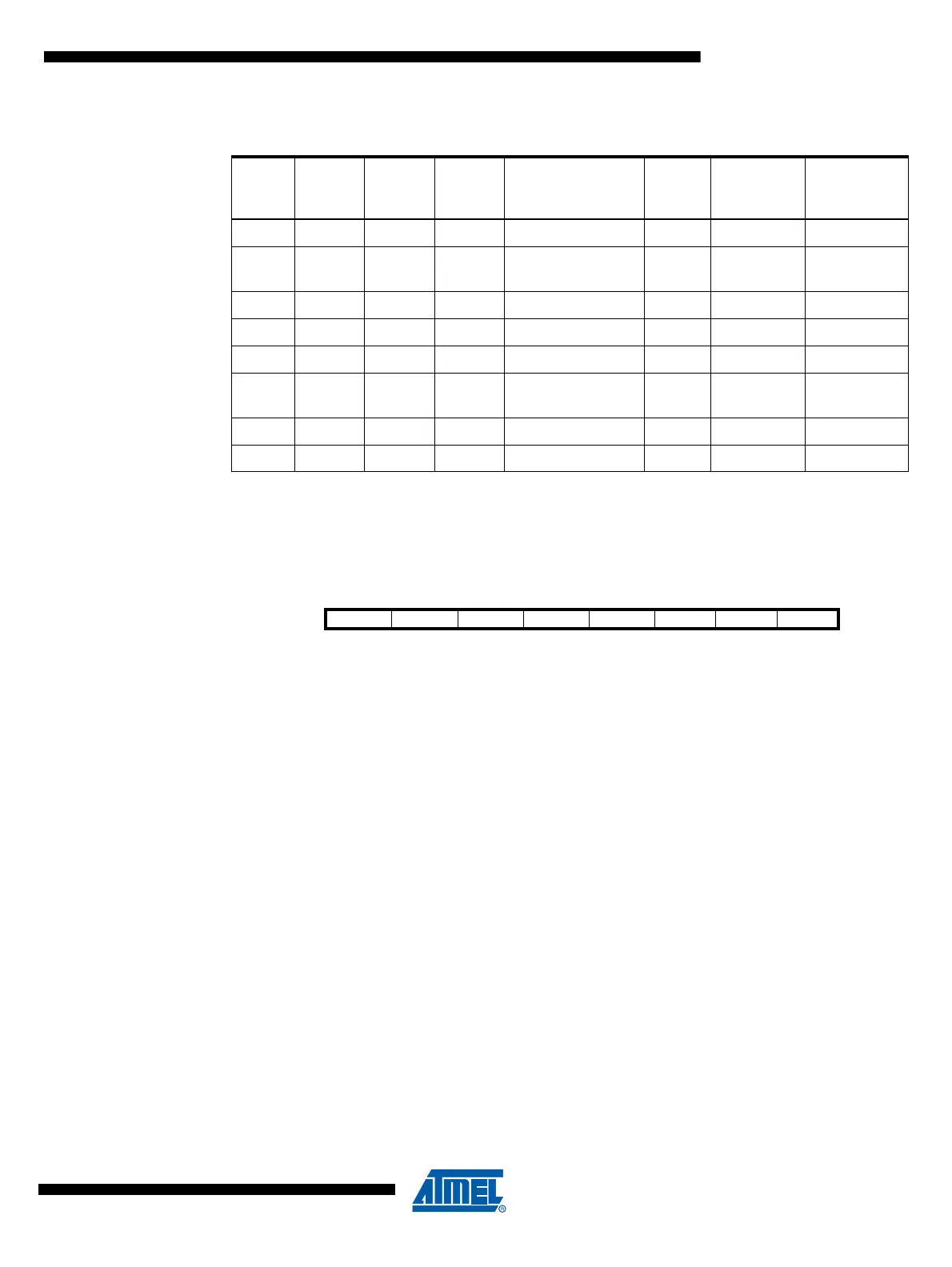
Notes: 1. MAX = 0xFF
2. BOTTOM = 0x00
12.8.2 Timer/Counter Control Register B – TCCR0B
• Bit 7 – FOC0A: Force Output Compare A
The FOC0A bit is only active when the WGM bits specify a non-PWM mode.
However, for ensuring compatibility with future devices, this bit must be set to zero when
TCCR0B is written when operating in PWM mode. When writing a logical one to the FOC0A bit,
an immediate Compare Match is forced on the Waveform Generation unit. The OC0A output is
changed according to its COM0A1:0 bits setting. Note that the FOC0A bit is implemented as a
strobe. Therefore it is the value present in the COM0A1:0 bits that determines the effect of the
forced compare.
A FOC0A strobe will not generate any interrupt, nor will it clear the timer in CTC mode using
OCR0A as TOP.
The FOC0A bit is always read as zero.
• Bit 6 – FOC0B: Force Output Compare B
The FOC0B bit is only active when the WGM bits specify a non-PWM mode.
However, for ensuring compatibility with future devices, this bit must be set to zero when
TCCR0B is written when operating in PWM mode. When writing a logical one to the FOC0B bit,
an immediate Compare Match is forced on the Waveform Generation unit. The OC0B output is
changed according to its COM0B1:0 bits setting. Note that the FOC0B bit is implemented as a
strobe. Therefore it is the value present in the COM0B1:0 bits that determines the effect of the
forced compare.
Table 12-7. Waveform Generation Mode Bit Description
Mode WGM2 WGM1 WGM0
Timer/Counter
Mode of
Operation TOP
Update of
OCRx at
TOV Flag
Set on
(1)(2)
0 0 0 0 Normal 0xFF Immediate MAX
10 0 1
PWM, Phase
Correct
0xFF TOP BOTTOM
2 0 1 0 CTC OCRA Immediate MAX
3 0 1 1 Fast PWM 0xFF TOP MAX
4 1 0 0 Reserved – – –
51 0 1
PWM, Phase
Correct
OCRA TOP BOTTOM
6 1 1 0 Reserved – – –
7 1 1 1 Fast PWM OCRA TOP TOP
Bit 7 6 5 4 3 2 1 0
FOC0A FOC0B – – WGM02 CS02 CS01 CS00 TCCR0B
Read/Write W W R R R/W R/W R/W R/W
Initial Value 0 0 0 0 0 0 0 0