EasyManua.ls Logo

Atmel ATtiny25 User Manual

Atmel ATtiny25
196 pages
To Next Page IconTo Next Page
To Previous Page IconTo Previous Page
Page #74 background imageLoading...
Page #74 background image
74
7598H–AVR–07/09
ATtiny25/45/85
Table 12-2 shows the COM0B1:0 bit functionality when the WGM02:0 bits are set to fast PWM
mode.
Note: 1. A special case occurs when OCR0B equals TOP and COM0B1 is set. In this case, the Com-
pare Match is ignored, but the set or clear is done at TOP. See “Fast PWM Mode” on page 67
for more details.
Table 12-3 shows the COM0B1:0 bit functionality when the WGM02:0 bits are set to phase cor-
rect PWM mode.
Note: 1. A special case occurs when OCR0B equals TOP and COM0B1 is set. In this case, the Com-
pare Match is ignored, but the set or clear is done at TOP. See “Phase Correct PWM Mode” on
page 69 for more details.
Bits 3, 2 – Res: Reserved Bits
These bits are reserved bits in the ATtiny25/45/85 and will always read as zero.
Bits 1:0 – WGM01:0: Waveform Generation Mode
Combined with the WGM02 bit found in the TCCR0B Register, these bits control the counting
sequence of the counter, the source for maximum (TOP) counter value, and what type of wave-
form generation to be used, see Table 12-7. Modes of operation supported by the Timer/Counter
unit are: Normal mode (counter), Clear Timer on Compare Match (CTC) mode, and two types of
Pulse Width Modulation (PWM) modes (see “Modes of Operation” on page 66).
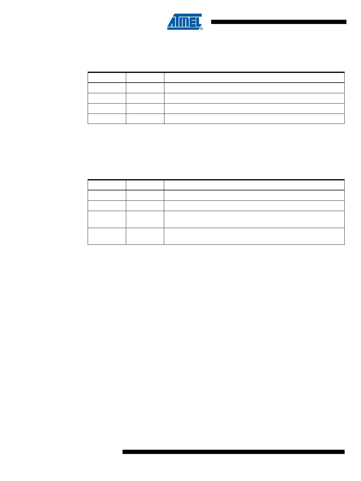
Table 12-5. Compare Output Mode, Fast PWM Mode
(1)
COM01 COM00 Description
0 0 Normal port operation, OC0B disconnected.
01Reserved
1 0 Clear OC0B on Compare Match, set OC0B at TOP
1 1 Set OC0B on Compare Match, clear OC0B at TOP
Table 12-6. Compare Output Mode, Phase Correct PWM Mode
(1)
COM0A1 COM0A0 Description
0 0 Normal port operation, OC0B disconnected.
01Reserved
10
Clear OC0B on Compare Match when up-counting. Set OC0B on
Compare Match when down-counting.
11
Set OC0B on Compare Match when up-counting. Clear OC0B on
Compare Match when down-counting.

Table of Contents

Question and Answer IconNeed help?

Do you have a question about the Atmel ATtiny25 and is the answer not in the manual?

Atmel ATtiny25 Specifications

General IconGeneral
ArchitectureAVR
Flash Memory2 KB
SRAM128 B
EEPROM128 B
Clock Speed20 MHz
I/O Pins6
PWM Channels2
Operating Voltage1.8V - 5.5V
ADC4 channels, 10-bit
Communication InterfacesSPI, I2C, USART
Operating Temperature Range-40°C to 85°C
Timers8-bit Timer/Counter with PWM, 16-bit Timer/Counter with PWM
Package8-pin PDIP, SOIC-8

Summary

Features

Overview and Pin Configurations

Pinout

Pin configuration details for ATtiny25/45/85, showing pin functions for SOIC and QFN packages.

Overview

Introduces the ATtiny25/45/85 as a low-power AVR microcontroller with RISC architecture.

AVR CPU Core

Architecture & Registers

Covers CPU core, architectural overview, ALU, status, and general purpose registers.

Instruction Execution & Reset/Interrupts

Details instruction timing, reset, and interrupt handling mechanisms.

ATtiny25/45/85 Memories

Flash, SRAM, EEPROM, and I/O Memory

Describes Flash, SRAM, EEPROM, and I/O memory spaces and their characteristics.

System Clock and Clock Options

Clock Sources and Prescalers

Details clock sources (RC, Crystal, PLL) and the system clock prescaler.

Power Management and Sleep Modes

MCU Control Register

Details the MCU Control Register for power management and sleep mode selection.

Sleep Modes (Idle, ADC Noise Reduction, Power-down)

Explains the different sleep modes and their features for power saving.

Power Reduction Register

Describes the PRR for stopping clocks to peripherals to reduce power consumption.

System Control and Reset

Reset Sources

Lists and describes the various reset sources like Power-on, External, Watchdog, and Brown-out.

Brown-out Detection

Details the On-chip Brown-out Detection (BOD) circuit and its configuration.

Interrupts

Interrupt Vectors in ATtiny25/45/85

Lists the interrupt vectors and their definitions for ATtiny25/45/85.

I/O Ports

Ports as General Digital I/O

Covers port configuration, general I/O, and switching between input/output.

Alternate Port Functions

Explains alternate functions of port pins and overriding signals.

Register Description for I/O-Ports

Details the PORTB, DDRB, and PINB registers for I/O port control.

External Interrupts

MCU Control Register – MCUCR

Details the External Interrupt Control Register for interrupt sense control.

General Interrupt Mask Register – GIMSK

Covers the GIMSK for enabling external and pin change interrupts.

8-bit Timer/Counter0 with PWM

Modes of Operation and Registers

Explains operational modes and register descriptions for Timer/Counter0.

Counter and Compare Units

Timer/Counter1 and Dead Time Generator

Details Timer/Counter1 operation and the Dead Time Generator for PWM.

Universal Serial Interface – USI

Functional Descriptions and Registers

Covers USI modes (3-wire, SPI, 2-wire) and register descriptions.

Analog Comparator

ACSR and ADCSRB Registers

Details Analog Comparator Control and Status Registers for configuration and interrupts.

Analog Comparator Multiplexed Input

Explains selecting ADC pins as the negative input to the Analog Comparator.

Analog to Digital Converter

ADC Features and Operation

Lists ADC features and describes its operation, including channel and reference selection.

Starting a Conversion

Explains manual and auto-triggered ADC conversion start methods.

ADC Conversion Result

Details how to read and interpret ADC conversion results in different modes.

debugWIRE On-chip Debug System

Features, Interface, and Registers

Covers debugwire features, physical interface, limitations, and registers.

Memory Programming

Lock Bits and Fuse Bytes

Explains memory lock bits and the functionality of fuse bytes.

Serial Downloading

Details serial programming methods including SPI and HVSP.

High-voltage Serial Programming

Covers programming Flash, EEPROM, Lock bits, and Fuse bits using HVSP.

Electrical Characteristics

Absolute Maximum Ratings*

Lists the stress ratings that may cause permanent damage to the device.

DC Characteristics

Provides DC characteristics across temperature and voltage ranges.

Typical Characteristics

Supply Current (Active, Idle, Power-down)

Shows supply current graphs for different modes versus frequency and VCC.

Pin Characteristics (Pull-up, Driver Strength, Thresholds)

Details pin pull-up, driver strength, and threshold characteristics.

Oscillator and BOD Characteristics

Covers BOD thresholds and internal oscillator frequency characteristics.

Register Summary

Instruction Set Summary

Ordering Information

Package Types

Lists available package types like T5 and PC with their specifications.

Document Revision History

Errata

Related product manuals