110
7598H–AVR–07/09
ATtiny25/45/85
17.3 Analog Comparator Multiplexed Input
It is possible to select any of the ADC3..0 pins to replace the negative input to the Analog Com-
parator. The ADC multiplexer is used to select this input, and consequently, the ADC must be
switched off to utilize this feature. If the Analog Comparator Multiplexer Enable bit (ACME in
ADCSRB) is set and the ADC is switched off (ADEN in ADCSRA is zero), MUX1..0 in ADMUX
select the input pin to replace the negative input to the Analog Comparator, as shown in Table
17-2. If ACME is cleared or ADEN is set, AIN1 is applied to the negative input to the Analog
Comparator.
17.3.1 Digital Input Disable Register 0 – DIDR0
• Bits 1, 0 – AIN1D, AIN0D: AIN1, AIN0 Digital Input Disable
When this bit is written logic one, the digital input buffer on the AIN1/0 pin is disabled. The corre-
sponding PIN Register bit will always read as zero when this bit is set. When an analog signal is
applied to the AIN1/0 pin and the digital input from this pin is not needed, this bit should be writ-
ten logic one to reduce power consumption in the digital input buffer.
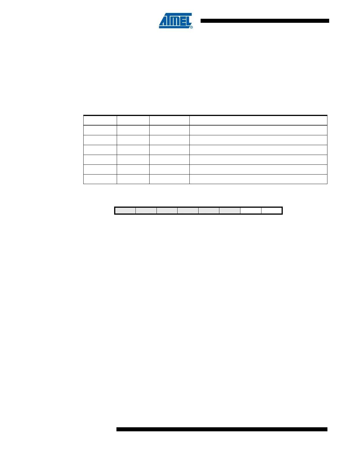
Table 17-2. Analog Comparator Multiplexed Input
ACME ADEN MUX1..0 Analog Comparator Negative Input
0x xxAIN1
11 xxAIN1
10 00ADC0
10 01ADC1
10 10ADC2
10 11ADC3
Bit 76543210
– – ADC0D ADC2D ADC3D ADC1D AIN1D AIN0D DIDR0
Read/Write R R R/W R/W R/W R/W R/W R/W
Initial Value00000000