58
7598H–AVR–07/09
ATtiny25/45/85
10.4 Register Description for I/O-Ports
10.4.1 Port B Data Register – PORTB
10.4.2 Port B Data Direction Register – DDRB
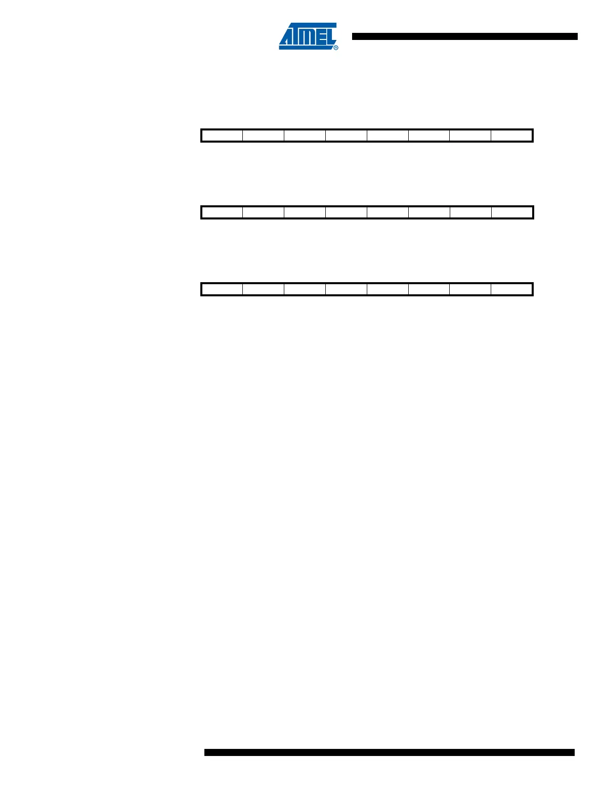
10.4.3 Port B Input Pins Address – PINB
11. External Interrupts
The External Interrupts are triggered by the INT0 pin or any of the PCINT5..0 pins. Observe that,
if enabled, the interrupts will trigger even if the INT0 or PCINT5..0 pins are configured as out-
puts. This feature provides a way of generating a software interrupt. Pin change interrupts PCI
will trigger if any enabled PCINT5..0 pin toggles. The PCMSK Register control which pins con-
tribute to the pin change interrupts. Pin change interrupts on PCINT5..0 are detected
asynchronously. This implies that these interrupts can be used for waking the part also from
sleep modes other than Idle mode.
The INT0 interrupts can be triggered by a falling or rising edge or a low level. This is set up as
indicated in the specification for the MCU Control Register – MCUCR. When the INT0 interrupt is
enabled and is configured as level triggered, the interrupt will trigger as long as the pin is held
low. Note that recognition of falling or rising edge interrupts on INT0 requires the presence of an
I/O clock, described in “Clock Systems and their Distribution” on page 21. Low level interrupt on
INT0 is detected asynchronously. This implies that this interrupt can be used for waking the part
also from sleep modes other than Idle mode. The I/O clock is halted in all sleep modes except
Idle mode.
Note that if a level triggered interrupt is used for wake-up from Power-down, the required level
must be held long enough for the MCU to complete the wake-up to trigger the level interrupt. If
the level disappears before the end of the Start-up Time, the MCU will still wake up, but no inter-
rupt will be generated. The start-up time is defined by the SUT and CKSEL Fuses as described
in “System Clock and Clock Options” on page 21.
Bit 76543210
– – PORTB5 PORTB4 PORTB3 PORTB2 PORTB1 PORTB0 PORTB
Read/Write R R R/W R/W R/W R/W R/W R/W
Initial Value 0 0 0 0 0 0 0 0
Bit 76543210
––
DDB5 DDB4 DDB3 DDB2 DDB1 DDB0 DDRB
Read/Write R R R/W R/W R/W R/W R/W R/W
Initial Value 0 0 0 0 0 0 0 0
Bit 76543210
––
PINB5 PINB4 PINB3 PINB2 PINB1 PINB0 PINB
Read/Write R R R/W R/W R/W R/W R/W R/W
Initial Value 0 0 N/A N/A N/A N/A N/A N/A