59
7598H–AVR–07/09
ATtiny25/45/85
11.1 MCU Control Register – MCUCR
The External Interrupt Control Register A contains control bits for interrupt sense control.
• Bits 1, 0 – ISC01, ISC00: Interrupt Sense Control 0 Bit 1 and Bit 0
The External Interrupt 0 is activated by the external pin INT0 if the SREG I-flag and the corre-
sponding interrupt mask are set. The level and edges on the external INT0 pin that activate the
interrupt are defined in Table 11-1. The value on the INT0 pin is sampled before detecting
edges. If edge or toggle interrupt is selected, pulses that last longer than one clock period will
generate an interrupt. Shorter pulses are not guaranteed to generate an interrupt. If low level
interrupt is selected, the low level must be held until the completion of the currently executing
instruction to generate an interrupt.
11.2 General Interrupt Mask Register – GIMSK
• Bits 7, 4..0 – Res: Reserved Bits
These bits are reserved bits in the ATtiny25/45/85 and will always read as zero.
• Bit 6 – INT0: External Interrupt Request 0 Enable
When the INT0 bit is set (one) and the I-bit in the Status Register (SREG) is set (one), the exter-
nal pin interrupt is enabled. The Interrupt Sense Control0 bits 1/0 (ISC01 and ISC00) in the MCU
Control Register (MCUCR) define whether the external interrupt is activated on rising and/or fall-
ing edge of the INT0 pin or level sensed. Activity on the pin will cause an interrupt request even
if INT0 is configured as an output. The corresponding interrupt of External Interrupt Request 0 is
executed from the INT0 Interrupt Vector.
• Bit 5 – PCIE: Pin Change Interrupt Enable
When the PCIE bit is set (one) and the I-bit in the Status Register (SREG) is set (one), pin
change interrupt is enabled. Any change on any enabled PCINT5..0 pin will cause an
interrupt. The corresponding interrupt of Pin Change Interrupt Request is executed from
the PCI Interrupt Vector. PCINT5..0 pins are enabled individually by the PCMSK0 Register.
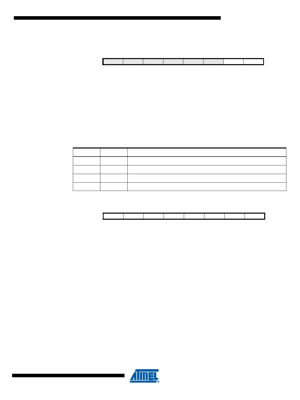
Bit 76543210
BODS PUD SE SM1 SM0 BODSE ISC01 ISC00 MCUCR
Read/Write R/W R/W R/W R/W R/W R/W R/W R/W
Initial Value00000000
Table 11-1. Interrupt 0 Sense Control
ISC01 ISC00 Description
0 0 The low level of INT0 generates an interrupt request.
0 1 Any logical change on INT0 generates an interrupt request.
1 0 The falling edge of INT0 generates an interrupt request.
1 1 The rising edge of INT0 generates an interrupt request.
Bit 76543210
–INT0PCIE–––––GIMSK
Read/Write R R/W R/W R R R R R
Initial Value 0 0 0 0 0 0 0 0