3
7598H–AVR–07/09
ATtiny25/45/85
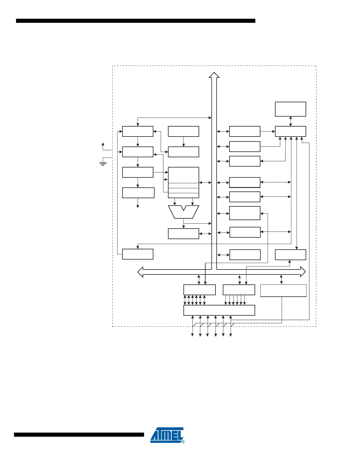
2.1 Block Diagram
Figure 2-1. Block Diagram
The AVR core combines a rich instruction set with 32 general purpose working registers. All the
32 registers are directly connected to the Arithmetic Logic Unit (ALU), allowing two independent
registers to be accessed in one single instruction executed in one clock cycle. The resulting
architecture is more code efficient while achieving throughputs up to ten times faster than con-
ventional CISC microcontrollers.
PROGRAM
COUNTER
INTERNAL
OSCILLA
TOR
WATCHDOG
TIMER
STACK
POINTER
PROGRAM
FLASH
SRAM
MCU CONTROL
REGISTER
GENERAL
PURPOSE
REGISTERS
INSTRUCTION
REGISTER
TIMER/
COUNTER0
SERIAL
UNIVERSAL
INTERFACE
TIMER/
COUNTER1
INSTRUCTION
DECODER
DATA DIR.
REG.PORT B
DATA REGISTER
PORT B
PROGRAMMING
LOGIC
TIMING AND
CONTROL
MCU STATUS
REGISTER
STATUS
REGISTER
ALU
PORT B DRIVERS
PB0-PB5
VCC
GND
CONTROL
LINES
8-BIT DATABUS
Z
ADC /
ANALOG COMPARATOR
INTERRUPT
UNIT
DATA
EEPROM
CALIBRATED
OSCILLATORS
Y
X
RESET