85
7598H–AVR–07/09
ATtiny25/45/85
The Stop condition provides a Timer Enable/Disable function.
14.1.2 General Timer/Counter1 Control Register - GTCCR
• Bit 6- PWM1B: Pulse Width Modulator B Enable
When set (one) this bit enables PWM mode based on comparator OCR1B in Timer/Counter1
and the counter value is reset to $00 in the CPU clock cycle after a compare match with OCR1C
register value.
• Bits 5,4 - COM1B1, COM1B0: Comparator B Output Mode, Bits 1 and 0
The COM1B1 and COM1B0 control bits determine any output pin action following a compare
match with compare register B in Timer/Counter1. Output pin actions affect pin PB3 (OC1B).
Since this is an alternative function to an I/O port, the corresponding direction control bit must be
set (one) in order to control an output pin. Note that OC1B
is not connected in normal mode.
In PWM mode, these bits have different functions. Refer to Table 14-4 on page 90 for a detailed
description.
0 1 1 1 PCK/64 CK/64
1 0 0 0 PCK/128 CK/128
1 0 0 1 PCK/256 CK/256
1 0 1 0 PCK/512 CK/512
1 0 1 1 PCK/1024 CK/1024
1 1 0 0 PCK/2048 CK/2048
1 1 0 1 PCK/4096 CK/4096
1 1 1 0 PCK/8192 CK/8192
1 1 1 1 PCK/16384 CK/16384
Table 14-2. Timer/Counter1 Prescale Select (Continued)
CS13 CS12 CS11 CS10
Asynchronous
Clocking Mode
Synchronous
Clocking Mode
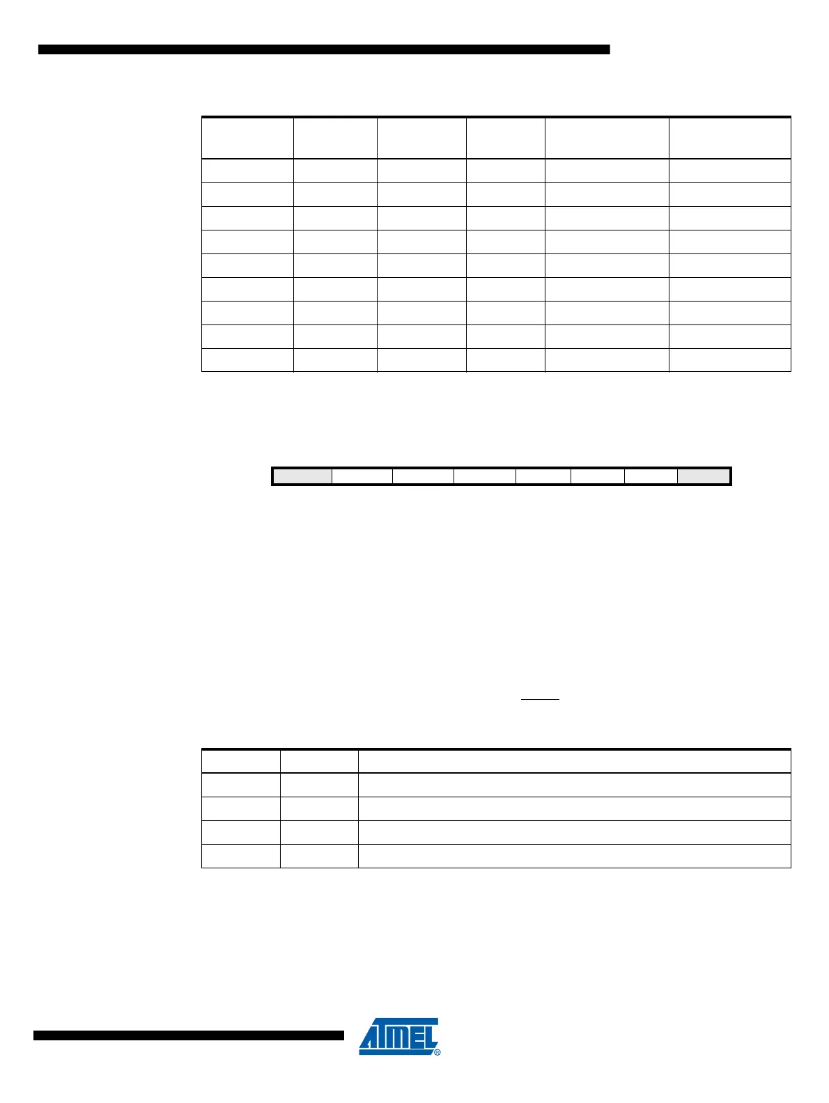
Bit 7 6 5 4 3 2 1 0
$2C ($4C)
TSM PWM1B COM1B1 COM1B0 FOC1B FOC1A PSR1 PSR0 GTCCR
Read/Write R/W R/W R/W R/W W W R/W R/W
Initial value 0 0 0 0 0 0 0 0
Table 14-3. Comparator B Mode Select
COM1B1 COM1B0 Description
0 0 Timer/Counter Comparator B disconnected from output pin OC1B.
0 1 Toggle the OC1B output line.
1 0 Clear the OC1B output line.
1 1 Set the OC1B output line