301
7679H–CAN–08/08
AT90CAN32/64/128
23.3.1 Bypass Register
The Bypass Register consists of a single Shift Register stage. When the Bypass Register is
selected as path between TDI and TDO, the register is reset to 0 when leaving the Capture-DR
controller state. The Bypass Register may be used to shorten the scan chain on a system when
the other devices are to be tested.
23.3.2 Device Identification Register
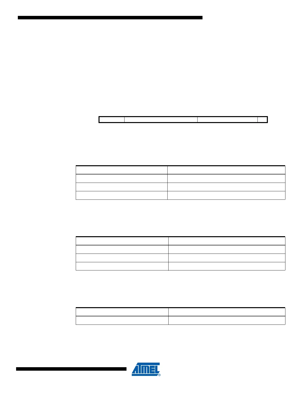
Figure 23-1 shows the structure of the Device Identification Register.
Figure 23-1. The Format of the Device Identification Register
23.3.2.1 Version
Version is a 4-bit number identifying the revision of the component. The relevant version number
is shown in Table 23-1.
23.3.2.2 Part Number
The part number is a 16-bit code identifying the component. The JTAG Part Number for
AT90CAN32/64/128 is listed in Table 23-2.
23.3.2.3 Manufacturer ID
The Manufacturer ID is a 11-bit code identifying the manufacturer. The JTAG manufacturer ID
for ATMEL is listed in Table 23-3.
MSB LSB
Bit 31 2827 1211 1 0
Device ID Version Part Number Manufacturer ID 1
4 bits 16 bits 11 bits 1-bit
Table 23-1. JTAG Version Numbers
Version JTAG Version Number (Hex)
AT90CAN32 revision A 0x0
AT90CAN64 revision A 0x0
AT90CAN128 revision A 0x0
Table 23-2. AVR JTAG Part Number
Part Number JTAG Part Number (Hex)
AT90CAN32 0x9581
AT90CAN64 0x9681
AT90CAN128 0x9781
Table 23-3. Manufacturer ID
Manufacturer JTAG Manufacturer ID (Hex)
ATMEL 0x01F

 Loading...


