36
AT90S2313
0839G–08/01
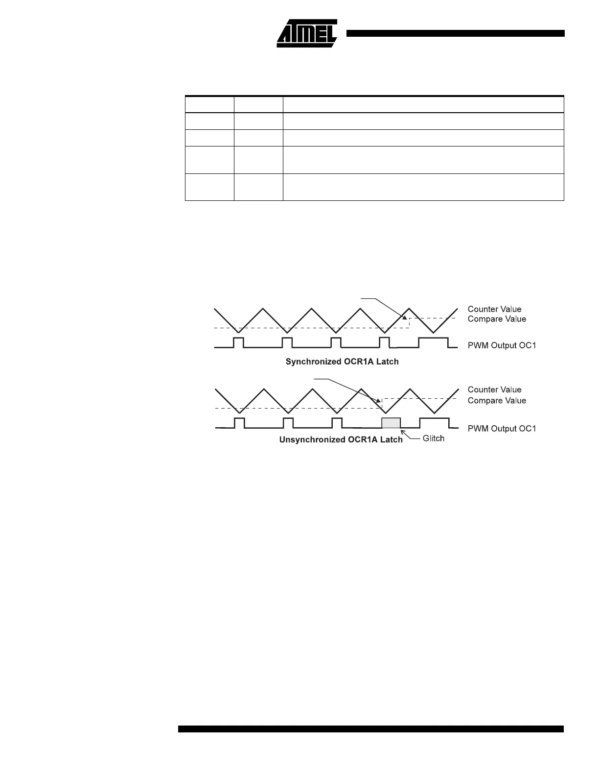
Note that in the PWM mode, the 10 least significant OCR1A bits, when written, are
transferred to a temporary location. They are latched when Timer/Counter1 reaches
TOP. This prevents the occurrence of odd-length PWM pulses (glitches) in the event of
an unsynchronized OCR1A write. See Figure 32 for an example.
Figure 32. Effects on Unsynchronized OCR1 Latching
During the time between the write and the latch operations, a read from OCR1A will
read the contents of the temporary location. This means that the most recently written
value always will read out of OCR1A.
When the OCR1 contains $0000 or TOP, the output OC1 is updated to low or high on
the next compare match according to the settings of COM1A1/COM1A0. This is shown
in Table 13.
Note: If the compare register contains the TOP value and the prescaler is not in use
(CS12..CS10 = 001), the PWM output will not produce any pulse at all, because the up-
counting and down-counting values are reached simultaneously. When the prescaler is
in use (CS12..CS10 ≠ 001 or 000), the PWM output goes active when the counter
reaches the TOP value, but the down-counting compare match is not interpreted to be
reached before the next time the counter reaches the TOP value, making a one-period
PWM pulse.
Table 12. Compare1 Mode Select in PWM Mode
COM1A1 COM1A0 Effect on OC1
0 0 Not connected
0 1 Not connected
10
Cleared on compare match, upcounting. Set on compare match,
down-counting (non-inverted PWM).
11
Cleared on compare match, downcounting. Set on compare match,
up-counting (inverted PWM).
Compare V
alue changes
Compare Value changes

 Loading...


