Clock Distribution
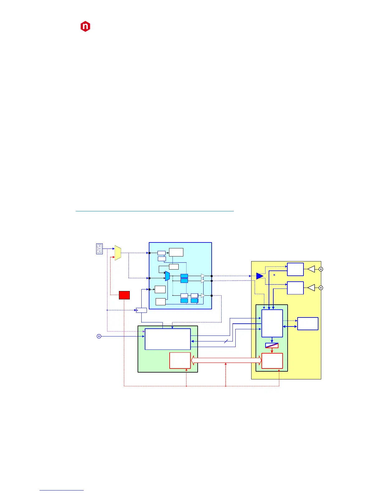
The module clock distribution takes place on two domains: OSC-CLK and REF-CLK; the former is a fixed 50MHz clock
provided by an on- board oscillator, the latter provides the ADC sampling clock.
OSC-CLK handles Local Bus (communication between motherboard and mezzanine boards; see red traces in Fig. 9.2).
REF-CLK handles ADC sampling, trigger logic, acquisition logic (samples storage into RAM, buffer freezing on trigger)
through a clock chain. Such domain can use either an external (via front panel signal on CLK-IN) or an internal (via local
oscillator) source; in the latter case, OSC-CLK and REF-CLK will be synchronous (the operation mode remains the same
anyway).
DT5730 and DT5725 use an integrated phase-locked-loop (PLL) and clock distribution device, AD9520. It is used to
generate the sampling clock for ADCs and the mezzanine FPGA (SAMP-CLK0/SAMP-CLK1), as well as the trigger logic
synchronization clock (TRG-CLK).
Both clocks can be generated from the internal oscillator (50 MHz) or from external clock input. By default, the board
uses the internal clock as PLL reference (REF-CLK).
The external clock can be selected by write access at register address 0x8100 (refer to [RD2]). The external clock signal
must be differential (LVDS, ECL, PECL, LVPECL, CML) with a jitter lower than 100ppm (see § Tab. 3.1).
AD9520 configuration can be changed and stored into non-volatile memory. Changing the AD9520 configuration is
primarily intended to be used for external PLL reference clock frequency change:
DT5730 and DT5725 lock to an external 50 MHz clock with default AD9520 configuration (see § PLL Mode).
Refer to the AD9520 datasheet for more details:
http://www.analog.com/static/imported-files/data_sheets/AD9520-3.pdf
(in case the active link above doesn’t work, copy and paste it on the internet browser)



 To Next Page