Electronic Instrumentation
UM3148 – DT5730/DT5725 User Manual rev. 2
3 Technical Specifications
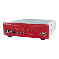
Form Factor 154x50x164 mm
3
(WxHxD) Desktop
Channels
8 channels
Single ended
Bandwidth
250 MHz (DT5730)
125 MHz (DT5725)
Full Scale Range
0.5 or 2 V
pp
(default)
SW selectable
Offset
Programmable 16-bit
DAC for DC offset
adjustment on each
channel.
Range: ±1 V (@2V
pp
);
±0.25 V (@0.5V
pp
)
Sampling Rate
500 MS/s Simultaneously on each channel (DT5730
250 MS/s Simultaneously on each channel (DT5725)
Clock source: internal/external
On-board programmable PLL provides generation of the main board clocks from an internal (50 MHz
local Oscillator) or external (front panel CLK-IN connector) reference
CLK-IN (AMP Modu II)
AC coupled differential input clock.
LVDS, ECL, PECL, LVPECL, CML
(single ended NIM/TTL available by CAEN
adapter)
Jitter<100ppm requested
TRG-IN (LEMO)
External trigger digital input
NIM/TTL, Z
in
= 50 Ω
GPO (LEMO)
General purpose digital output
NIM/TTL, R
t
= 50 Ω
GPI (LEMO)
General purpose digital input
NIM/TTL, Z
in
= 50 Ω
640 kS/ch or 5.12 MS/s Multi-event Buffer divisible into 1 ÷ 1024 buffers
Independent read and write access; programmable event size and pre/post-trigger
Trigger Source
Self-trigger: channel over/under-
threshold for Common or Individual (DPP
firmware only) Trigger generation
External-trigger: Common trigger by
TRG-IN connector
Software-trigger: Common trigger by
software command
Trigger Propagation
GPO programmable digital output
Trigger Time Stamp
Default FW: 31-bit counter, 16 ns resolution, 17 s range;
48-bit extension available by firmware
DPP-PHA/DPP-PSD FW (DT5730): 31-bit counter, 2 ns
resolution, 4 s range; 47-bit extension available by
firmware; 10-bit and 2 ps fine time stamp by digital CFD
(DPP-PSD FW only); 64-bit extension available by software
DPP-PHA/DPP-PSD FW (DT5725): 31-bit counter, 4 ns
resolution, 8 s range; 47-bit extension available by
firmware; 10-bit and 4 ps fine time stamp by digital CFD
(DPP-PSD FW only); 64-bit extension available by software
Clock Propagation
One-to-many: clock distribution from an
external clock source on CLK-IN
connector
Acquisition Synchronization
Sync, Start/Stop through digital I/O (TRG-IN or GPI input,
GPO output)
Trigger Time Stamps Alignment
By GPI input connector
Altera Cyclone EP4CE30 (one FPGA serves 4 channels)
Optical Link
CAEN CONET proprietary protocol
Up to 80 MB/s transfer rate
Daisy chainable: it is possible to
connect up to 8 or 32 ADC modules to a
single Optical Link Controller
(respectively A2818 or A3818)
USB
USB 2.0 compliant
Up to 30 MB/s transfer rate
DPP-PSD for the Pulse Shape Discrimination (e.g. Neutron-Gamma discrimination)
DPP-PHA for the Pulse Height Analysis
Firmware can be upgraded via USB/Optical Link
General purpose C libraries, configuration tools, readout software (Windows and Linux support)
Tab. 3.1: Specifications table