CONTENTS
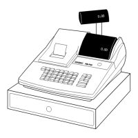
FE-700 Page
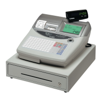
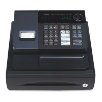
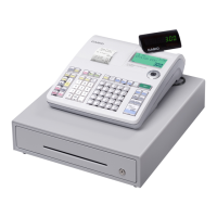
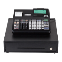
1. SPECIFICATIONS........................................................................................ 1
2. INITIALIZE (MAC) OPERATION.................................................................. 2
3. F-INIT (FMAC) OPERATION ....................................................................... 2
4. BLOCK DIAGRAM....................................................................................... 3
4-1. PCB CONNECTION.............................................................................. 3
4-2. BLOCK DIAGRAM (CIRCUIT).............................................................. 4
5. DISASSEMBLY (FE-700)............................................................................. 5
5-1. MAIN PARTS ........................................................................................ 5
6. CIRCUIT EXPLANATION ............................................................................ 8
6-1. Power supply circuit ........................................................................... 8
6-2. CPU (IC11: uPD78052GC-A46-8BT) ................................................... 9
6-3. Display controller (IC2: uPD16312GB-3B4)..................................... 11
6-4. Initilize IC (Reset circuit)................................................................... 12
6-5. Power down detection circuit (PWD)............................................... 12
6-6. Address latch circuit ......................................................................... 12
6-7. RAM / ROM / Fiscal ROM bank selection circuit............................. 13
6-8. Fiscal ROM address and data selection.......................................... 14
6-9. Head drive circuit for printer ............................................................ 15
6-10. VPP sensor circuit........................................................................... 16
6-11. Power supply circuit for display ................................................... 17
7. DIAGNOSTIC ............................................................................................. 18
7-1. To start the diagnostic program ...................................................... 18
7-2. Check item ......................................................................................... 18
7-3. Operation of each test....................................................................... 18
7-4. Switch status test .............................................................................. 19
7-5. Individual function test ..................................................................... 20
7-6. Fiscal ROM test.................................................................................. 23
7-7. To exit the diagnostic test ................................................................ 23
8. ERROR CODE ........................................................................................... 24
8-1. Operation error code......................................................................... 24
8-2. Fiscal ROM error code ...................................................................... 25
8-3. System lock code .............................................................................. 26
9. IC DATA ..................................................................................................... 27
10. PCB LAYOUT ............................................................................................ 32
11. CIRCUIT DIAGRAM ................................................................................... 33
12. PARTS LIST............................................................................................... 50