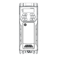
Unidrive SP Low Voltage DC Installation Guide 15
Issue Number: 1 www.controltechniques.com
Safety Information Introduction Product information
System design
Component data Index
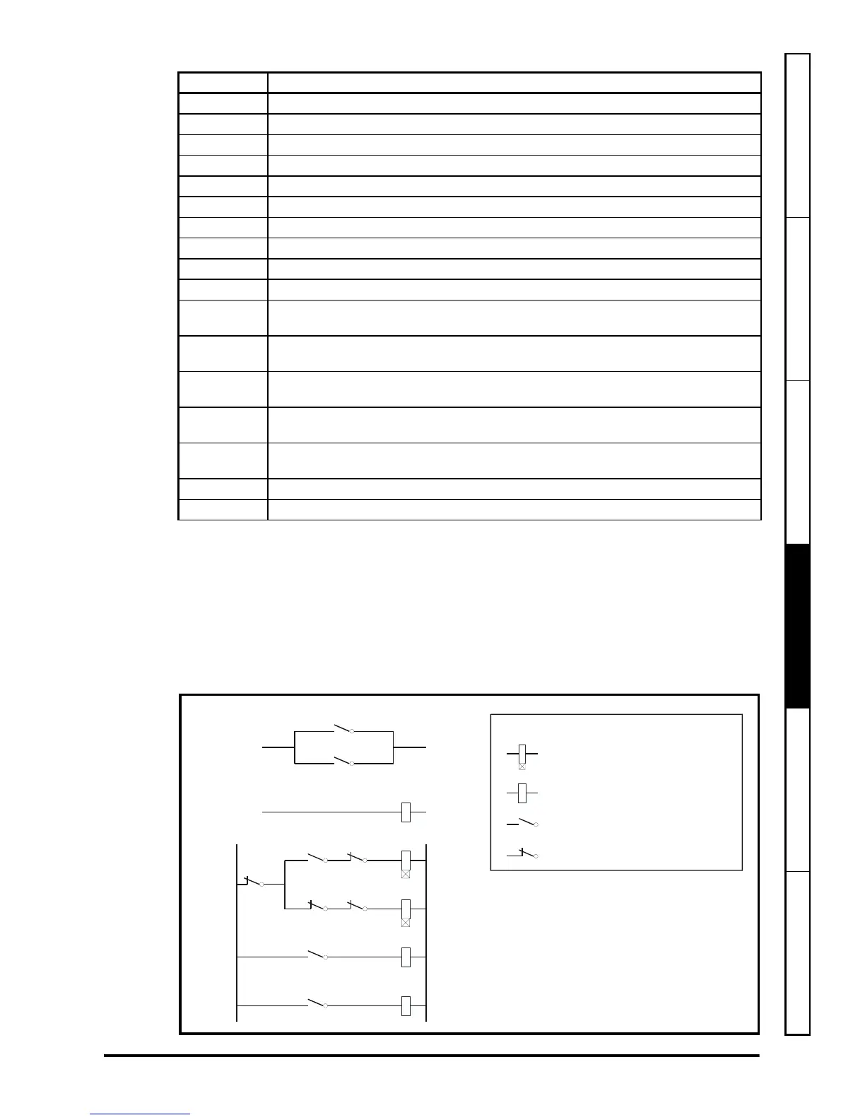
Table 4-2 Key for Figure 4-1
4.6.2 Control implementation for system configuration 1
In order to achieve the required Low Voltage DC operation sequencing as detailed in
section 4.7 Power circuit control logic and sequencing on page 24. The circuitry shown
in Figure 4-1 and Figure 4-2 below are required.
Some of the circuitry shown in Figure 4-2 can be reduced by using SM-Applications, this
is further discussed in section 4.7.2 Control implementation using SM-Applications on
page 26.
Figure 4-2 Control circuitry for system configuration 1
Key Description
Aux.1 Ovld.1 auxillary contact
C1 DC supply capacitor (SP1 only)
D1 Blocking diode to prevent energy from being returned to the LVDC supply
Ovld.1 Thermal overload relay to protect the discharge resistor
F1a 3 phase AC supply fusing
F2a Fuse for LVDC supply feed to drive +DC terminal
F2b Fuse for LVDC supply feed to drive -DC terminal
F2c Fuse for LVDC supply feed to drive 48V terminal
F3 Fuse for drive control 24V external input
K1 Normally open contacts supplying the drive with 3 phase AC when energized
K1b
Normally closed contacts that bring in the discharge resistor when the AC supply is
removed
K2a
Normally open contact, which when closed supplies the drive with the positive feed
from the LVDC power supply
K2b
Normally open contact, which when closed supplies the drive with the negative feed
from the LVDC power supply
K2c
Normally open contacts which when closed supply the 48V terminal of the drive
with LVDC
K2d
Normally closed contacts that bring in the discharge resistor when the DC supply is
removed
PS1 LVDC power supply
Rdis DC bus discharge resistor