PIN
DESCRIPTION
NO. NAME I/O
5-V
TOLERANT
34 RST I Yes Reset Input, active low(2) (4)
35 RXIN1 I Ye s Biphase signal, input 1, built-in coaxial amplier
36 VDDRX – – Power supply, 3.3 V (typ.), for RXIN0 and RXIN1.
37 RXIN0 I Ye s Biphase signal, input 0, built-in coaxial amplier
38 GNDRX - - Ground, for RXIN
39 XTI I No Oscillation circuit input for crystal resonator or external XTI clock source input(5)
40 XTO O No Oscillation circuit output for crystal resonator
41 AGND – – Ground, for PLL analog
42 VCC – – Power supply, 3.3 V (typ.), for PLL analog
43 FILT O No External PLL loop lter connection terminal; must connect recommended lter
44 VCOM O No ADC common voltage output; must connect external decoupling capacitor
45 AGNDAD – – Ground, for ADC analog
46 VCCAD – – Power supply, 5.0 V (typ.), for ADC analog
47 VINL I No ADC analog voltage input, left channel
48 VINR I No ADC analog voltage input, right channel
(1) Schmitt trigger input
(2) Schmitt trigger input
(3) Open-drain conguration in I2C mode
(4) Onboard pull-down resistor (50 kΩ, typical)
(5) CMOS Schmitt trigger input
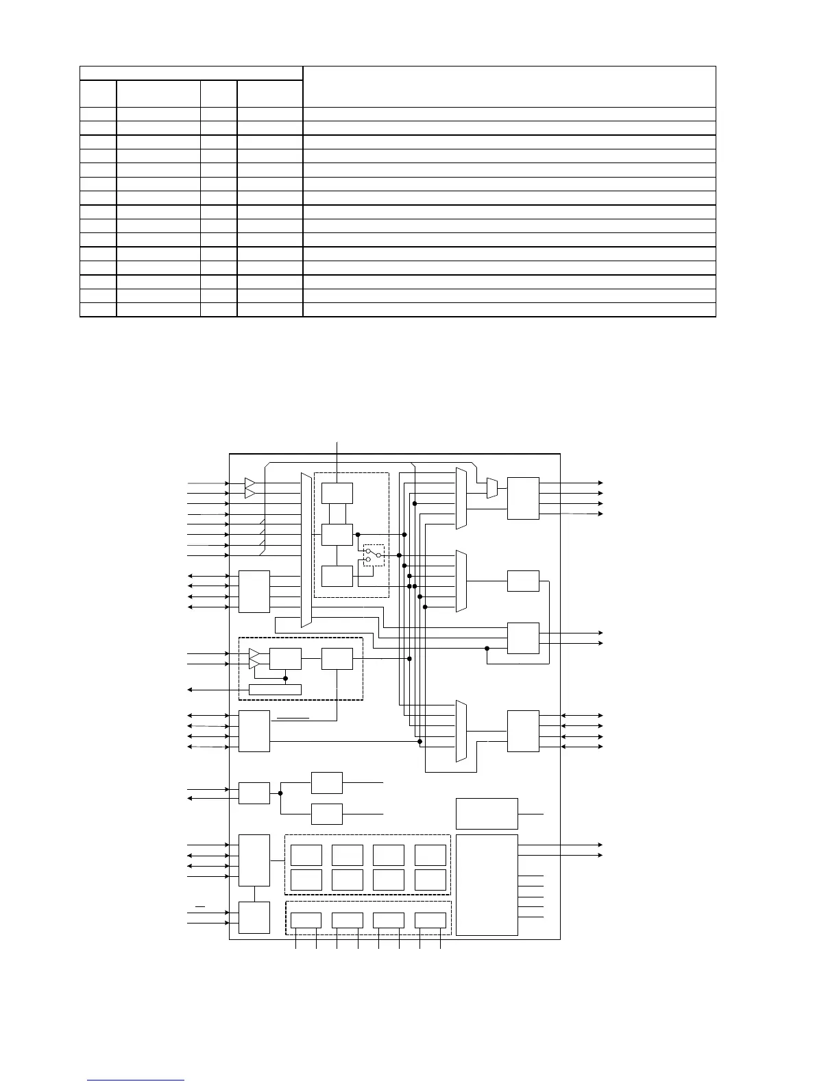
PCM9211 BLOCK DIAGRAM
Clock/ Data
Recovery
MPIO_A
SELECTOR
MPIO_C
SELECTOR
MPIO _B
SELECTOR
ADC
Com. Supply
MPO0/1
SELECTOR
MPO 0
MPO 1
MAIN
OUTPUT
SCKO
BCK
LRCK
DOUT
PORT
RXIN8
RXIN9
RXIN10
RXIN11
DITOUT
AUTO
DIR
ADC
AUXIN0
AUXIN1
AUXIN2
AUTO
DIR
ADC
AUXIN0
AUXIN1
AUXIN2
AUTO
DIR
ADC
AUXIN0
AUXIN1
DIT
Lock:DIR
Unlock:ADC
AUXIN 2
AUXOUT
OSC
Divider
XMCKO
Divider
XMCKO
DITOUT
RECOUT0
RECOUT1
AUXIN 0
AUXIN1
ADC Standalone
ADC Mode
Control
Function
Control
REGISTER
POWER SUPPLY
MC /SCL
MDI /SDA
MDO /ADR 0
MS/ADR 1
 Loading...