T5L_ASIC Development Guide
D
WI
N
T
echnology
Pro
f
essional
,
Credi
t
able
,
Success
f
ul
(5) When porting code from standard C or other 8051 platforms, users should be aware that the
SFR header file should be loaded with the T5L compliant .INC or .H file during compilation. If the
SFR definition in the customer code is different from the T5L definition, you can modify the code or
the T5L SFR header file to keep the same.
(6)HME05 realizes hardware simulation by downloading code to Code RAM of T5L OS CPU. The
code is not burned to Flash in the chip. To burn code into the chip, it is necessary to use SD card
interface or UART1 debugging interface. During SD card download, T5L underlying software will
automatically change the location of OS code 0x00F8 to 0x0000 (JMARK interface is forbidden) 44 57
49 4E 54 35.
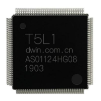
T5L OS CPU adopts the standard 8051 architecture. Except for the slight difference between SFR
and extended peripheral access, the instruction set is identical.
When porting the user's original 8051 code, it can be done quickly by taking care of the following
aspects.
(1) According to the hardware design, after reset, the startup.A51 (C51 startup code) or initcpu ()
program provided by DWIN is used to simply modify and configure T5L-specific SFR and parameter
settings.
Typical differences are in IO, main frequency of timer, baud rate, interrupt, WDT, etc.
(2) T5L IO output mode is controllable. When switching between input and output modes, PxMDOUT
registers should be configured accordingly, otherwise errors will occur.
(3) Turn off interrupt embedding. EA = 0 for each interrupt service program and EA=1when exiting.
(4) When using off-chip RAM (XRAM) as data storage in the code, note that the starting address of
T5L 32KB data RAM should start at 0x8000.
(5) Code 0x00F8 position plus 0xFFFF (or 0x0000 forbid JMARK interface) 44 57 49 4E 54 35. (6)
Optimize the algorithm of the original code with MDU hardware computing acceleration; move the UI
and Internet (e.g., access to DWIN cloud through DWIN WiFi module) functions to DGUS II platform,
user code can be processed by simply reading and writing DGUS variable space, which can
significantly improve product performance and enhance R&D efficiency.

 Loading...