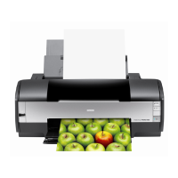
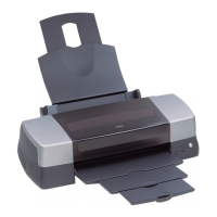
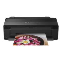
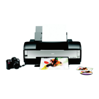
EPSON Stylus Photo 1390/1400/1410 Revision B
OPERATING PRINCIPLES Electrical Circuit Operating Principles 38
The following is the block diagram of the C655 MAIN control board.
Figure 2-14. C655 MAIN Control Board Block Diagram
CPU-ASIC
2 in 1
(IC9)
Data
Address
PROM
(IC6)
SDRAM
(IC7)
USB2.0
CN1
Motor
Driver
(IC11)
Head
Driver
(IC10)
Q6, Q9,
Q10, Q11
CN6
PF Encoder Sensor
Printhead
CR Encoder Sensor
CR Motor
CN5
CN15
CN4
C653 Head Board
C589 PSB/PSE Board
RTC
(IC8)
CN14
PW Sensor
DAC
(IC4)
Motor
Driver
(IC12)
PF Motor
APG Motor
ASF Motor
Pump Motor
CN3
Relay Board
PE Sensor
ASF Sensor
APG Sensor 1
APG Sensor 2
CN10
CN11
CN12
CN7
CN8
CN9
CN13
C589 Panel Board
CD-R Sensor
USB Host
CN2
The Stylus Photo 1390 does not have the following unit
and part shown in the boxes:
• USB Host CN2
•CD-R Sensor
 Loading...
