Hardware Description
ComTec GmbH 3-1
3. Hardware Description
3.1. Signal description of the 25-pin ADC connector
Sub-D male pin layout
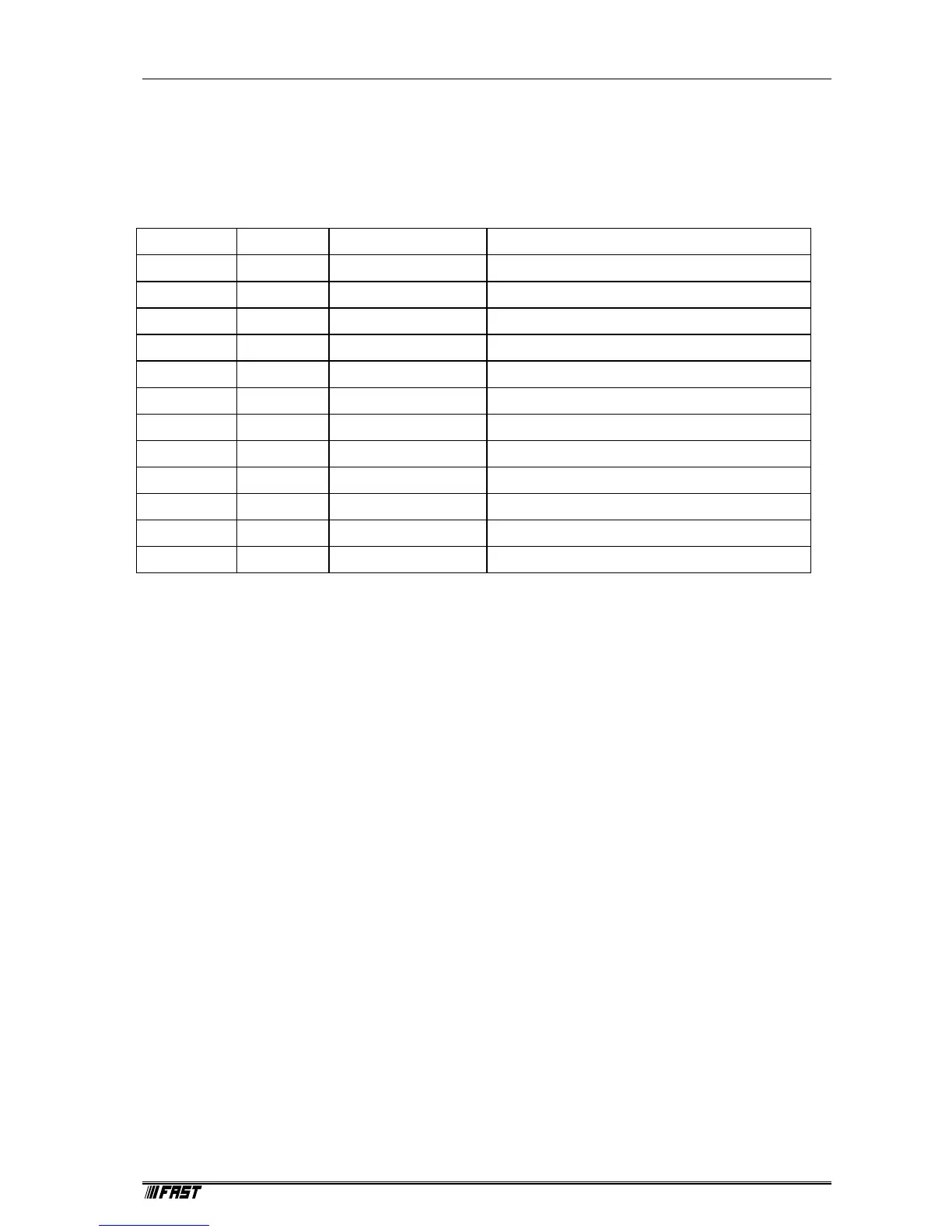
Pin Direction Mnemonic Signal
1-12 In D[0-12] Inverted Data D0-D12
13 In *DRDY Inverted Data Ready
14,15 In D13,D14 Inverted Data D13, D14
17 Out *ACC Data Accepted
18 Out *STOP Stop ADC
19 In D15 Inverted Data D15
20 In INH Inhibit, Drop Data
21 In DTIME Dead Time
22 Out *DEN Inverted Data Bus Enable
23 Out DWELL Dwell
24 Pwr GND Signal Ground
25 - E5V Do not connect
Signal Description
*D0-*D15 16 Bit inverted ADC data input.
Datalines are terminated with 2K2 pull-up Resistor against 5 Volt internal webMCA
supply. Therefore, inactive line state is approximate 5 Volt. Signal level is inverted, i.e.
logic level 0xffff means ADC signal value 0.
*DRDY Data Ready handshake signal from ADC.
Signal level inverted, active low asserted. If data on D[0-15] are setup the ADC should
assert this signal to denote valid data available. DRDY must be negated immediately
after *ACC is asserted.
*ACC Data Accepted handshake from webMCA.
Signal level inverted, active low asserted. If the ADC asserts DRDY, after latching the
data the webMCA asserts this Signal to denote data taken. The webMCA will not
respond with ACC if the internal FIFO buffer signals full state. The data transfer is
pending until FIFO buffer is available. ACC will immediately negate after DRDY is
negated.
INH Data Inhibit from ADC. If INH is sampled asserted high the current ADC data will be
ignored. The transfer cycle handshake proceeds.
*DEN Data Bus enable output. Always asserted low, will not be switched.
DWELL Dwell output to an MCS device, not used for the ADC interface. High asserted signals
to switch to the next bin.
DTIME Deadtime signal from ADC. If asserted high stops counting the Livetime.
GND Signal Ground.
E5V Do not connect, provides test voltage to external test circuit.