Reproduction forbidden without Fibocom Wireless Inc. written authorization - All Rights Reserved.
FM350-GL Hardware Guide Page 33 of 67
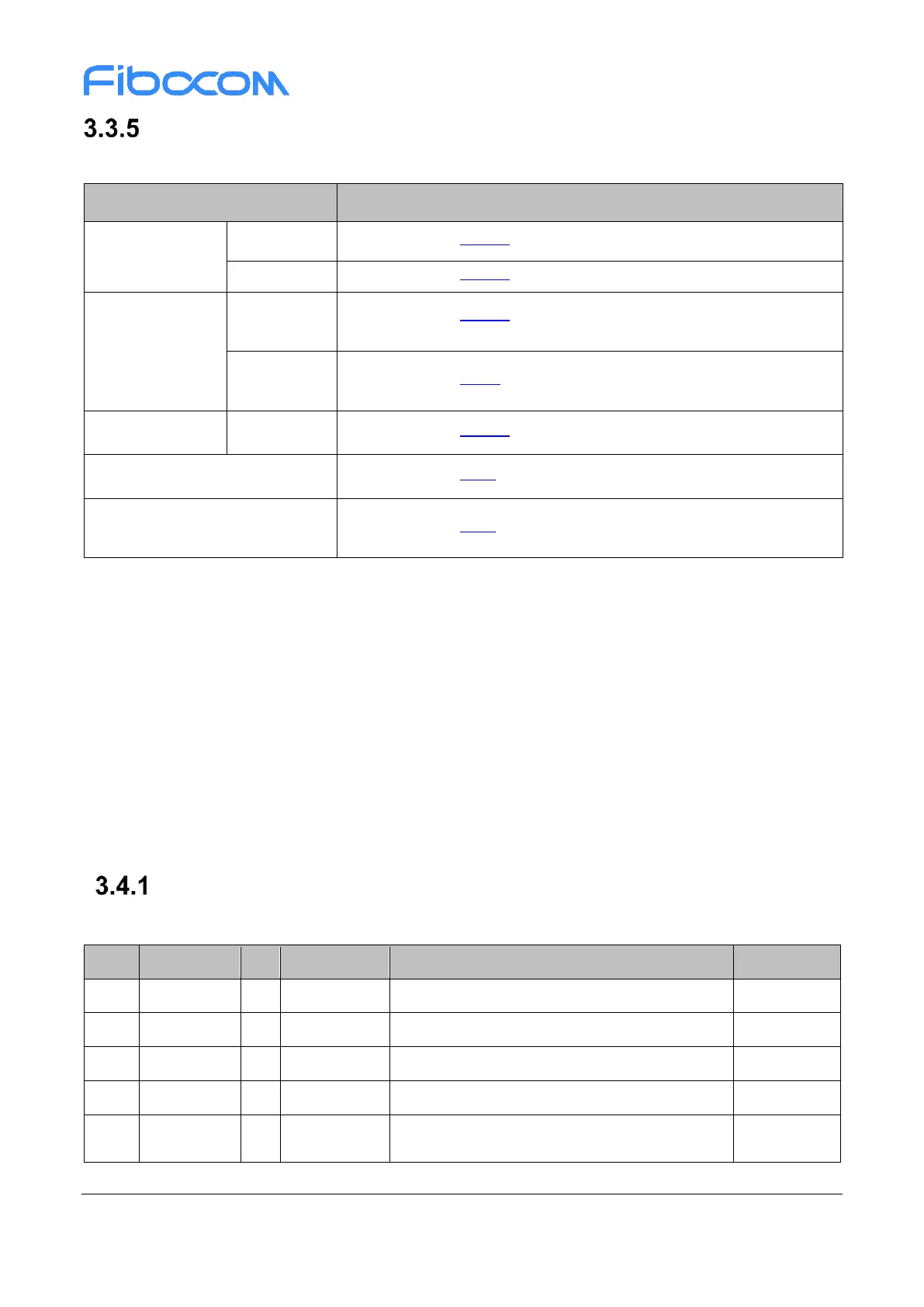
Timing Application
The recommended timing application in Win10 OS is as below table:
Refer to section 3.3.4.1 Figure 3-10 D0 L1.2 Timing
Refer to section 3.3.4.2 Figure 3-11/3-12 D3
cold
L2 timing
Refer to section 3.3.1.2 Figure 3-5 Timing control for start-up
Refer to section 3.3.2 Figure 3-6 Software power off timing
Refer to section 3.3.1.2 Figure 3-5 Timing control for start-up
Refer to section 3.3.3 Figure 3-9 Reset timing 2
nd
Modem FW upgrade / Modem
recovery
Refer to section 3.3.3 Figure 3-8 Reset timing 1
st
3.4 PCIe Interface
FM350 module supports PCIe as IPC interface for data transfer. The PCIe supports Gen3, one lane for
data transmission channel, it is also compatible with PCIe Gen2 and Gen1. BIOS configuration must follow
X86 platform BKC (Best Know Configuration) reference design.
PCIe interface initialized with host driver, then mapped MBIM & GNSS port in Win10 OS and RMNET &
AT port in Chrome/Linux/Android OS. The MBIM and RMNET interfaces are used for data transfer, GNSS
port is used for receiving GNSS data, AT port is used for AT command.
PCIe Interface Definition
PCIe interface is defined as below table:
PCIe TX Differential signals, negative
PCIe TX Differential signals, positive
PCIe RX Differential signals, negative
PCIe RX Differential signals, positive
PCIe Reference Clock signal
Negative
 Loading...