Reproduction forbidden without Fibocom Wireless Inc. written authorization - All Rights Reserved.
FM350-GL Hardware Guide Page 34 of 67
PCIe Reference Clock signal
Positive
Asserted to reset module PCIe interface
default. If module went into coredump, it will
reset whole module, not only PCIe interface.
Active low, internal pull up(10KΩ)
Asserted by device to request a PCIe
reference clock be available (active clock
state) in order to transmit data. It also used by
L1 PM Sub states mechanism, asserted by
either host or device to initiate an L1 exit.
Active low, open drain output and should add
external pull up on platform
Asserted to wake up system and reactivate
PCIe link from L2 to L0, it depends on system
whether supports wake up functionality.
Active low, open drain output and should add
external pull up on platform
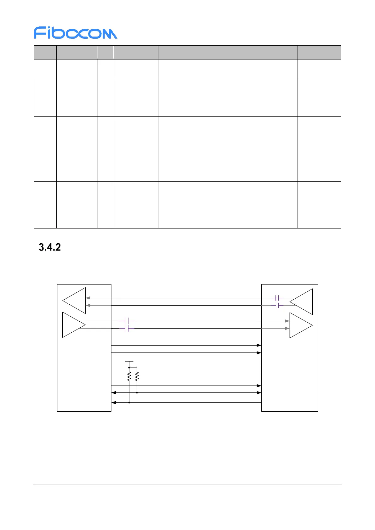
PCIe Interface Application
The reference circuit is shown in Figure 3-13:
ModuleAP
220nF
220nF
PERST#(pin50)
CLKREQ#(pin52)
PEWAKE#(pin54)
+3.3V/1.8V
100K
10K
TX
RX
RX
TX
220nF
220nF
41 PETn0
43 PETp0
47 PERn0
49 PERp0
REFCLKN(pin53)
REFCLKP(pin55)
PCIE_CLK_N
PCIE_CLK_P
PCIE_RX_N
PCIE_RX_P
PCIE_TX_N
PCIE_TX_P
PCIE_RST_N
PCIE_CLKREQ_N
PCIE_WAKE_N
Figure 3-13 Reference Circuit for PCIe Interface
FM350 module supports PCIe Gen3/one lane, including three difference pairs: transmit pair TXP/N,
receiving pair RXP/N and clock pair CLKP/N.
PCIe can achieve the maximum transmission rate of 8 GT/s, and must strictly follow the rules below in
PCB Layout:
 Loading...