pin 8 of the ADCs (U23, U22, U21, U20) should be at least
0.2 V above the lower limit and that the highest voltage pulse
on any pin 8 of the ADCs should be at least 0.3 V below the
upper limit. If an interpolator has a voltage pulse outside the
limi ts the measurement result will be wrong. Figure cc shows
the signals on an ADC.
The signal from the prescaler is connected to pin 22 (sin
-
gle-ended) of U11. It comes via a level converter. Check the
input signal to the converter at R335 (PECL levels).
If the FPGA or a part in the interpolators has been changed or
repaired, a calibration of internals must be performed after
-
wards. See Chapter 7.
Note The interpolator design has varied slightly in the
course of time, but the pulses in Figures 6-49 and
6-50 are very little affected.
6-28 Troubleshooting
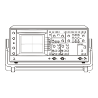
Figure 6-48 Important locations for the measuring logic.
R623
X4
X3
U11 U20
U21
U23
R335
U22
Figure 6-49 ADC 10461 behavior. Time A-A, 10 MHz in.
U21:8
U20:8
U22:8
U23:8