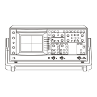
voltages. The range is 14.9 V to 17.5 V measured at X1 on the
display board. Set the contrast so X1 is 16.2 V. Check the
LCD voltages at X2 (14.7 V), X3 (13.3 V), X4 (2.9 V) and X5
(1.5 V). See Figure 6-72.
The FPGA (U11) is programmed by the processor. The used
pins are PROGN, INITN, DONE (X65), Clock and Data. See
Figure 6-75. The loading starts when PROGN is set low. Then
the processor checks that INITN is low and sets PROGN high
again. The FPGA responds by setting DONE low. After load
-
ing, which takes approximatel y 1.4 s, the FPGA sets DONE
high (check X65), if the loading was successful. If an error is
detected, INITN is set low. One clock pulse after DONE is set
high, all I/Os on the FPGA are defined. If the loading of the
FPGA is not successful, the program just goes on with the rest
of the startup procedure. At test point X67 the FPGA will out
-
put approximately 14 Hz. This signal shows that the FPGA is
working and will be switched off about 8 minutes after
power-up.
The fan is set to 8.4 V. Measure on J19 or J28. The input am
-
plifiers are initialized and a "click" from the relays is heard.
The I
2
C bus is used for controlling the relays.
Note: The I
2
C bus is of the utmost importance for the start of
the instrument. The keys, the LCD and the relays in
the input amplifiers all need a faultless I
2
C bus to work
properly.
Note: If the Flash PROM is exchanged, it must be replaced
by a preprogrammed Flash PROM. Voltage and
timebase calibration must be performed anew. The
utility program must be used for transferring the cali
-
bration results to new factory calibrations. The serial
number and the oscillator option must also be pro-
grammed by the utility program.
6-44 Troubleshooting
Figure 6-71 Important locations on PCB 1 during startup.
J19
J28
U39
X33X66
X31
X55
X67
X30
X28
X29
X65
R358
Figure 6-72 Important locations on PCB 2 during startup.
X3
X2
X5
X1
R33
U3
R34
X4