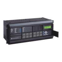
B-18 T60 Transformer Protection System GE Multilin
B.4 MEMORY MAPPING APPENDIX B
B
1D02 Source 1 Negative Watthour 0 to 1000000000000 Wh 0.001 F060 0
1D04 Source 1 Positive Varhour 0 to 1000000000000 varh 0.001 F060 0
1D06 Source 1 Negative Varhour 0 to 1000000000000 varh 0.001 F060 0
1D08 Reserved (8 items) --- --- --- F001 0
1D10 ...Repeated for Source 2
1D20 ...Repeated for Source 3
1D30 ...Repeated for Source 4
1D40 ...Repeated for Source 5
1D50 ...Repeated for Source 6
Energy Commands (Read/Write Command)
1D60 Energy Clear Command 0 to 1 --- 1 F126 0 (No)
Source Frequency (Read Only) (6 Modules)
1D80 Frequency for Source 1 2 to 90 Hz 0.001 F003 0
1D82 Frequency for Source 2 2 to 90 Hz 0.001 F003 0
1D84 Frequency for Source 3 2 to 90 Hz 0.001 F003 0
1D86 Frequency for Source 4 2 to 90 Hz 0.001 F003 0
1D88 Frequency for Source 5 2 to 90 Hz 0.001 F003 0
1D8A Frequency for Source 6 2 to 90 Hz 0.001 F003 0
Source Demand (Read Only) (6 Modules)
1E00 Source 1 Demand Ia 0 to 999999.999 A 0.001 F060 0
1E02 Source 1 Demand Ib 0 to 999999.999 A 0.001 F060 0
1E04 Source 1 Demand Ic 0 to 999999.999 A 0.001 F060 0
1E06 Source 1 Demand Watt 0 to 999999.999 W 0.001 F060 0
1E08 Source 1 Demand Var 0 to 999999.999 var 0.001 F060 0
1E0A Source 1 Demand Va 0 to 999999.999 VA 0.001 F060 0
1E0C Reserved (4 items) --- --- --- F001 0
1E10 ...Repeated for Source 2
1E20 ...Repeated for Source 3
1E30 ...Repeated for Source 4
1E40 ...Repeated for Source 5
1E50 ...Repeated for Source 6
Source Demand Peaks (Read Only Non-Volatile) (6 Modules)
1E80 Source 1 Demand Ia Maximum 0 to 999999.999 A 0.001 F060 0
1E82 Source 1 Demand Ia Maximum Date 0 to 4294967295 --- 1 F050 0
1E84 Source 1 Demand Ib Maximum 0 to 999999.999 A 0.001 F060 0
1E86 Source 1 Demand Ib Maximum Date 0 to 4294967295 --- 1 F050 0
1E88 Source 1 Demand Ic Maximum 0 to 999999.999 A 0.001 F060 0
1E8A Source 1 Demand Ic Maximum Date 0 to 4294967295 --- 1 F050 0
1E8C Source 1 Demand Watt Maximum 0 to 999999.999 W 0.001 F060 0
1E8E Source 1 Demand Watt Maximum Date 0 to 4294967295 --- 1 F050 0
1E90 Source 1 Demand Var 0 to 999999.999 var 0.001 F060 0
1E92 Source 1 Demand Var Maximum Date 0 to 4294967295 --- 1 F050 0
1E94 Source 1 Demand Va Maximum 0 to 999999.999 VA 0.001 F060 0
1E96 Source 1 Demand Va Maximum Date 0 to 4294967295 --- 1 F050 0
1E98 Reserved (8 items) --- --- --- F001 0
1EA0 ...Repeated for Source 2
1EC0 ...Repeated for Source 3
1EE0 ...Repeated for Source 4
1F00 ...Repeated for Source 5
1F20 ...Repeated for Source 6
Breaker Flashover (Read/Write Setting) (2 Modules)
2196 Breaker Flashover 1 Function 0 to 1 --- 1 F102 0 (Disabled)
2197 Breaker Flashover 1 Side 1 Source 0 to 5 --- 1 F167 0 (SRC 1)
2198 Breaker Flashover 1 Side 2 Source 0 to 6 --- 1 F211 0 (None)
Table B–10: MODBUS MEMORY MAP (Sheet 10 of 74)
ADDR REGISTER NAME RANGE UNITS STEP FORMAT DEFAULT