Ch.587
—————— Wiring procedure ——————
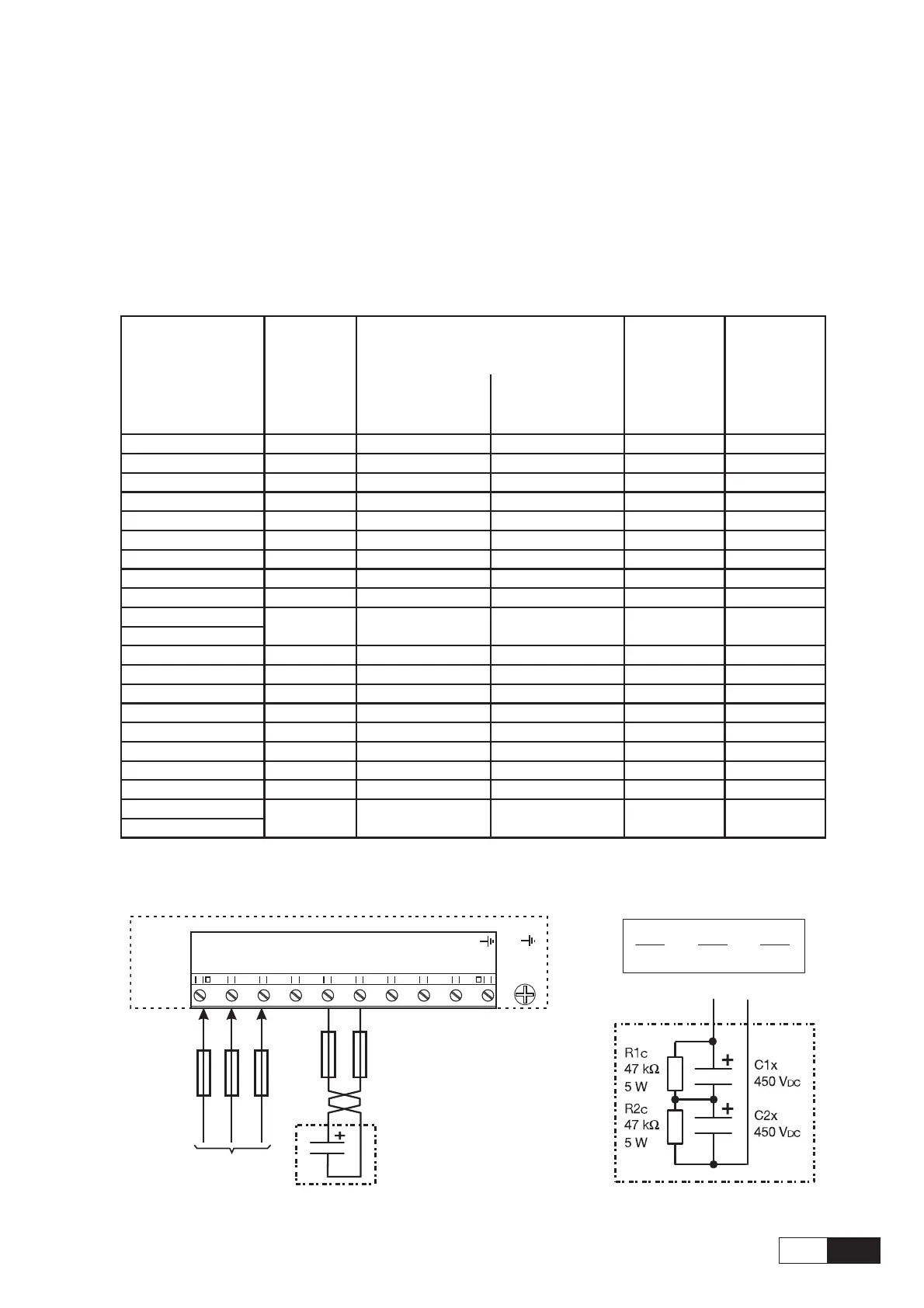
5.9. BUFFERING THE REGULATOR SUPPLY
The power supply of the control section is provided by a switched mode power supply unit (SMPS) from the
DC Link circuit. The Drive is disabled as soon as the voltage of the DC Link circuit is below the threshold
value (U
Buff
). The regulator supply is buffered by the energy of the DC Link circuit until the limit value (U
min
)
is reached. The buffer time is determined by the capacitance of the DC Link capacitors. The minimum
values are shown in the table below. The buffer time (t
Buff
) can be extended (only from 11 kW drive and
higher) by connecting external capacitors in parallel (on terminal C and D).
Table 5.9.1: DC Link Buffer Time
Internal Buffer time t
Buff
Maximum Maximum
capacitance (minimum value) with the permissible power required
Inverter type internal capacitance at : external by switched
AC Input AC Input capacitance mode power
C
std
voltage =400V voltage =460V supply
[µF][s][s] C
ext
[µF] P
SMPS
[W]
1007
220 0.165 0.25 0 65
1015
220 0.165 0.25 0 65
1022
330 0.24 0.37 0 65
1030
330 0.24 0.37 0 65
2040
830 0.62 0.95 0 65
2055
830 0.62 0.95 0 65
2075
830 0.62 0.95 0 65
3110
1500 1.12 1.72 1500 65
3150
1500 1.12 1.72 1500 65
4185
4220
4300
2200 1.88 2.8
4500 70
4370
3300 2.83 4.2
4500 70
5450 4950 4.24 6.3 4500 70
5550 4950 4.24 6.3 4500 70
6750 6600 5.6 8.1 0 70
7900 6600 5.6 8.1 0 70
71100
9900 8.4 12.1
070
71320 14100 12.8 17.2 0 70
81600
82000
avy4220
SMPS = Switched Mode Power Supply
70
14100 12.8 17.2 0 70
1800 1.54 2.3 4500
3Ph~
PE1 /
U1/L1
V1/L2
W1/L3
BR1
U2/T1
V2/T2
W2/T3
C
D
PE2/
F1
1
C
x
1
C1
x
1
C2
x
=+
C 900 V or
X DC
Figure 5.9.1: Buffering the Regulator Supply by Means of Additional Intermediate Circuit Capacitors