Rev. 1.30 7 of 34 November 13, 2020
e-Link32/e-Link32 Pro User’s Guide
1 Overview
1 Overview
Hardware Description
The e-Link32/e-Link32 Pro supports a Serial Wire Mode interface. There are only two pins,
SWCLK (Serial Wire Clock) and SWDIO (Serial Wire Debug Data Input/Output), which are used
for programming and debugging. However there are another two USB Virtual COM Ports for the
e-Link32 Pro Serial Communication
(Note)
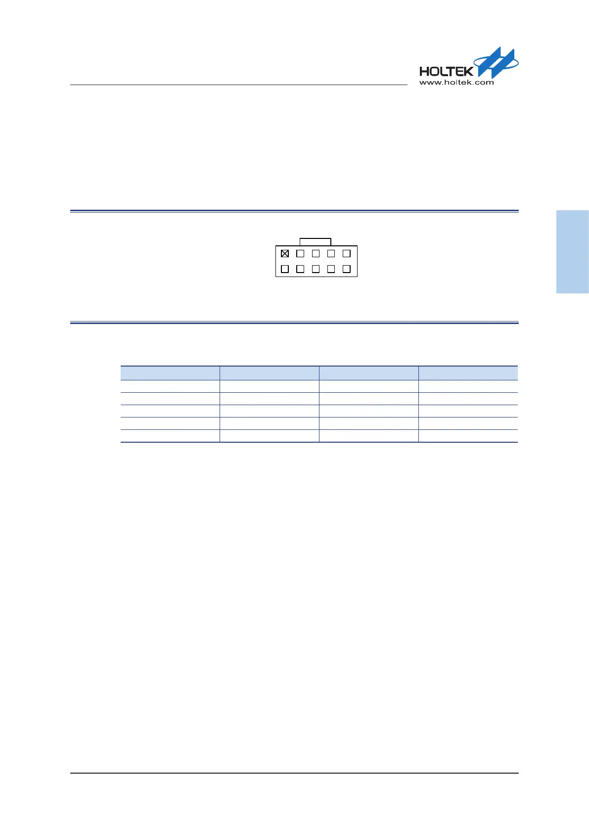
. The following illustration shows the debug connector.
2 84 6 10
1 7 9
3
5
Figure 2. SWD 10-Pin Connector
Table 1. SWD 10-Pin Connector Pins
Pin# Description Pin# Description
1 3.3V 2 SWDIO
3 GND 4 SWCLK
5 GND 6 Reserved
7 NC (VCOM_RXD
(Note)
) 8 NC (VCOM_TXD
(Note)
)
9 GND 10 Reset
Note: The serial communication function is only available for the e-Link32 Pro, Pin7 and Pin8 are NC
pins for the e-Link32.
Hardware Conguration
As the MCU has a wide operating voltage range, the SWD and other interface IO voltages of
the MCU may be different from the e-Link32/e-Link32 Pro which both operate at 3.3V. To
accommodate this problem a Level Shifter is integrated within the e-Link32/e-Link32 Pro to
handle dierent voltage level situations. However, users can also use dierent power supply modes
according to their various target board circuits and application purposes. For example:
▄
SWD/RESET/UART interface voltage determined by the target board power supply (hardware
factory default value):
The VDD power supply on the SWD interface is supplied by the target board. The SWD, RESET
and UART interface IO voltages of the e-Link32/e-Link32 Pro will be processed by the Level
Shifter to ensure that their voltage level is the same as the target board.
▄
MCU with independent IO power supply:
The SWD interface voltage is dierent from the RESET signal. For example, the SWD interface
operates at 1.8V while the RESET signal operates at 3.3V.