Section IV Model 204B
Paragraphs
4-11
to 4-15
Figure
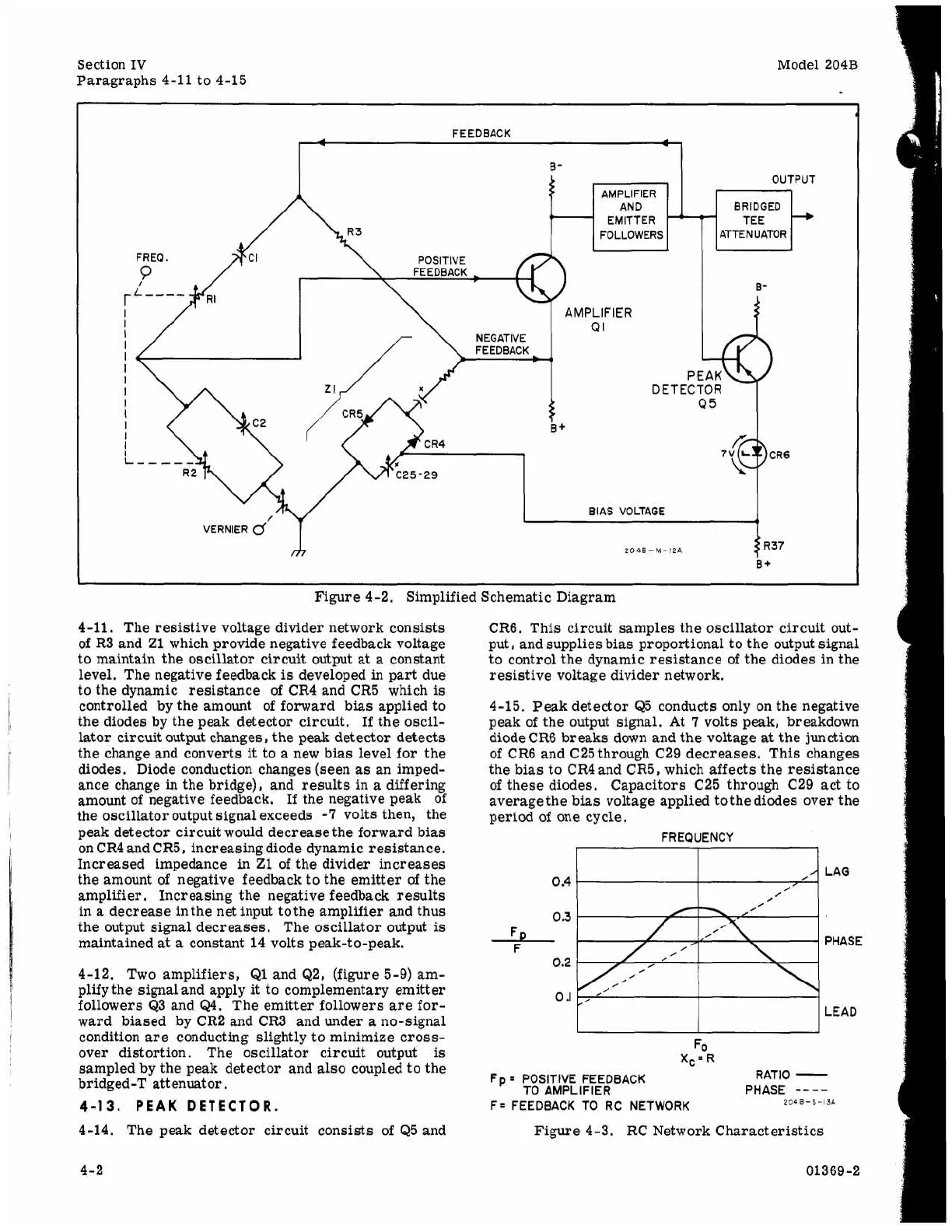
4-2.
Simplified Schematic Diagram
4-11. The resistive voltage divider network consists
of R3 and
Z1
which provide negative feedback voltage
to maintain the oscillator circuit output
at
a
constant
level. The negative feedback
is
developed
in
part due
to the dynamic resistance
of
CR4 and CR5 which
is
controlled by the amount of forward
bias
applied to
the diodes by the peak detector circuit. If the oscil-
lator circuit output changes,
the
peak detector detects
the change and converts
it
to
a
new bias level for the
diodes. Diode conduction changes (seen
as
an imped-
ance change in the bridge), and results in
a
differing
amount of negative feedback,
If
the negative peak of
the oscillator output signal exceeds
-7
volts then, the
peak detector circuit would decrease the forward
bias
on CR4 and
CR5,
increasing diode dynamic resistance.
Increased impedance in
Z1
of
the
divider increases
the amount of negative feedback to the emitter
of
the
amplifier. Increasing the negative feedback results
in
a
decrease in the net input tothe amplifier and thus
the output signal decreases. The oscillator output
is
maintained
at a
constant
14
volts peak-to-peak.
4-12.
Two amplifiers, Q1 and Q2, (figure 5-9) am-
plify the signal and apply
it
to complementary emitter
followers Q3 and
Q4.
The emitter followers are for-
ward biased by CR2 and CR3 and under
a
no-signal
condition are conducting slightly to minimize cross-
over distortion. The oscillator circuit output
is
sampled by the peak detector and also coupled to the
bridged-T attenuator.
4-14.
The peak detector circuit consists of Q5 and
4-13.
PEAK
DETECTOR.
CR6. This circuit samples the oscillator circuit out-
put, and supplies
bias
proportional to the output signal
to control the dynamic resistance of the diodes in the
resistive voltage divider network.
4-15. Peak detector Q5 conducts only on the negative
peak of the output signal. At
7
volts peak, breakdown
diode CR6 breaks down and the voltage
at
the junction
of CR6 and C25 through C29 decreases. This changes
the
bias
to CR4 and CR5, which affects the resistance
of these diodes. Capacitors C25 through C29 act to
averagethe
bias
voltage applied tothe diodes over the
period of one cycle.
FREQUENCY
0
A
0.3
F
0.2
0
R
LAG
PHASE
LEAD
RATIO
-
POSITIVE FEEDBACK
TO AMPLIFIER
FEEDBACK
TO
RC NETWORK
PHASE
204
0-S
-13A
Figure 4-3. RC Network Characteristics
4-2
01369-2