Intel® Xeon™ Processor with 800 MHz System Bus
Datasheet 17
2.5 Reserved or Unused Pins
All Reserved pins must remain unconnected. Connection of these pins to V
CC
, V
TT
, V
SS
, or to any
other signal (including each other) can result in component malfunction or incompatibility with
future processors. See Section 5.0 for a pin listing of the processor and the location of all Reserved
pins.
For reliable operation, always connect unused inputs or bidirectional signals to an appropriate
signal level. In a system level design, on-die termination has been included by the processor to
allow end agents to be terminated within the processor silicon for most signals. In this context, end
agent refers to the bus agent that resides on either end of the daisy-chained front side bus interface
while a middle agent is any bus agent in between the two end agents. For end agents, most unused
AGTL+ inputs should be left as no connects as AGTL+ termination is provided on the processor
silicon. However, see Table 6 for details on AGTL+ signals that do not include on-die termination.
For middle agents, the on-die termination must be disabled, so the platform must ensure that
unused AGTL+ input signals which do not connect to end agents are connected to V
TT
via a pull-
up resistor. Unused active high inputs, should be connected through a resistor to ground (V
SS
).
Unused outputs can be left unconnected, however this may interfere with some TAP functions,
complicate debug probing, and prevent boundary scan testing. A resistor must be used when tying
bidirectional signals to power or ground. When tying any signal to power or ground, a resistor will
also allow for system testability. Resistor values should be within ± 20% of the impedance of the
baseboard trace for front side bus signals. For unused AGTL+ input or I/O signals, use pull-up
resistors of the same value as the on-die termination resistors (R
TT
).
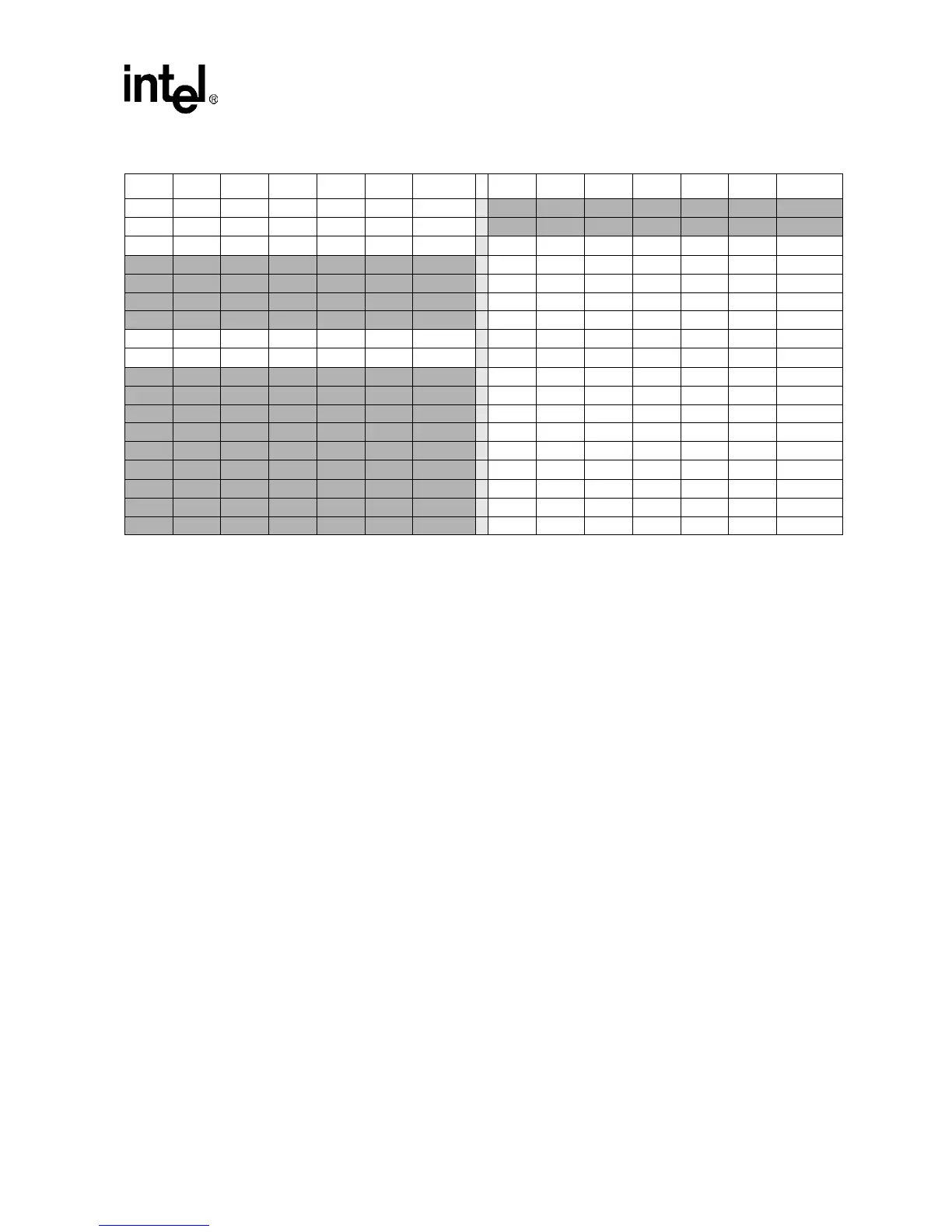
0 0 0 0 1 1 1.0125 0 1 0 0 1 1 1.3875
1 0 0 0 1 0 1.0250
1 1 0 0 1 0 1.4000
0 0 0 0 1 0 1.0375
0 1 0 0 1 0 1.4125
1 0 0 0 0 1 1.0500 1 1 0 0 0 1 1.4250
0 0 0 0 0 1 1.0625 0 1 0 0 0 1 1.4375
1 0 0 0 0 0 1.0750 1 1 0 0 0 0 1.4500
0 0 0 0 0 0 1.0875 0 1 0 0 0 0 1.4625
111111OFF
1
1 0 1 1 1 1 1.4750
011111OFF
1
0 0 1 1 1 1 1.4875
1 1 1 1 1 0 1.1000 1 0 1 1 1 0 1.5000
0 1 1 1 1 0 1.1125 0 0 1 1 1 0 1.5125
1 1 1 1 0 1 1.1250 1 0 1 1 0 1 1.5250
0 1 1 1 0 1 1.1375 0 0 1 1 0 1 1.5375
1 1 1 1 0 0 1.1500 1 0 1 1 0 0 1.5500
0 1 1 1 0 0 1.1625 0 0 1 1 0 0 1.5625
1 1 1 0 1 1 1.1750 1 0 1 0 1 1 1.5750
0 1 1 0 1 1 1.1875 0 0 1 0 1 1 1.5875
1 1 1 0 1 0 1.2000 1 0 1 0 1 0 1.6000
NOTES:
1. When this VID pattern is observed, the voltage regulator output should be disabled.
2. Shading denotes the expected default VID range during normal operation for Intel® Xeon™ processor with 800 MHz system
bus [1.2875 V -1.4000 V]. Please note this is subject to change.
3. Shaded areas do not represent the entire range of VIDs that may be driven by the processor. Events causing dynamic VID
transitions (see Section 2.4) may result in a more broad range of VID values.
Table 4. Voltage Identification Definition (Sheet 2 of 2)
2,3
VID5 VID4 VID3 VID2 VID1 VID0 V
CC_MAX
VID5 VID4 VID3 VID2 VID1 VID0 V
CC_MAX