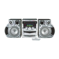
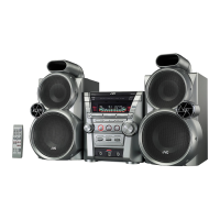
MX-GA77
1-30
3. Pin function (1/2)
-
-
-
I/O
I/O
I/O
I/O
I/O
O
O
I/O
I/O
Pin name
Power supply (-)
Power supply (+)
Test pin
Set as VSS with the user’s option. (see Note 1)
• 8bit input/output port
• Data direction programmable in nibble units
• Use of pull-up resistor can be specified in nibble units
• Input for HOLD release
• Input for port 0 interrupt
• 15V withstand at N-channel open drain output
• 8bit input/output port
• Data direction programmable for each bit
• Use of pull-up resistor can be specified for each bit
• Other pin functions
P10: SIO0 data output
P11: SIO0 data input / bus input / output
P12: SIO0 clock input / output
P13: SIO1 data output
P14: SIO1 data input / bus input / output
P15: SIO1 clock input / output
P16: Timer 1 PWML output
P17: Timer 1 PWMH output / Buzzer output
• 8bit input/output port
• Data direction can be specified for each bit
• Use of pull-up resistor can be specified for each bit
• 15V withstand at N-channel open drain output
• Other functions:
P30 to P33: INT4 input / HOLD release input / Timer 1 event input / Timer 0L
capture input / Timer 0H capture input
P34 to P37: INT5 input / HOLD release input / Timer 1 event input / Timer 0L
capture input / Timer 0H capture input
• 4bit input/output port
• Data direction can be specified for each bit
• Use of pull-up resistor can be specified for each bit
• Other functions
P70: INT0 input / HOLD release input / Timer0L capture input / Output for watchdog timer
P71: INT1 input / HOLD release input / Timer0H capture input
P72: INT2 input / HOLD release input / Timer 0 event input / Timer0L capture input
/ High speed clock counter input
P73: INT3 input(noise rejection filter attached input) / Timer 0 event input
/ Timer 0H capture input
AD input port: AN8(P70), AN9(P71), AN12(P72), AN13(P73)
• 8bit input/output port
• Input/output can be specified in a bit unit
• Other functions:
AD input port: AN0 to AN7
Weak signal detector input port: MICIN(P87)
• Large current output for VFD display controller digit (can be used for segment)
• Large current output for VFD display controller segment/digit
• Output for VFD display controller segment/digit
• Other functions:
High voltage input port: PC0 to PC7
• Output for VFD display controller segment
• Other functions:
High voltage input port: PD0 to PD7
Function I/O
VSS1, 2
VDD1,2,3,4
FIX0
PORT0
P00 to P07
PORT1
P10 to P17
PORT3
P30 to P37
PORT7
P70 to P73
PORT8
P80 to P87
S0/T0 to
S8/T8
S9/T9 to
S15/T15
S16 to S23
S24 to S31