1-37
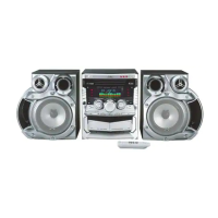
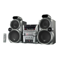
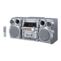
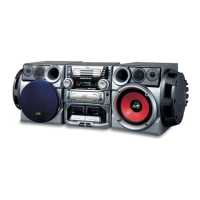
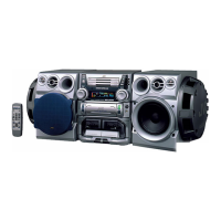
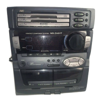
MX-GA77
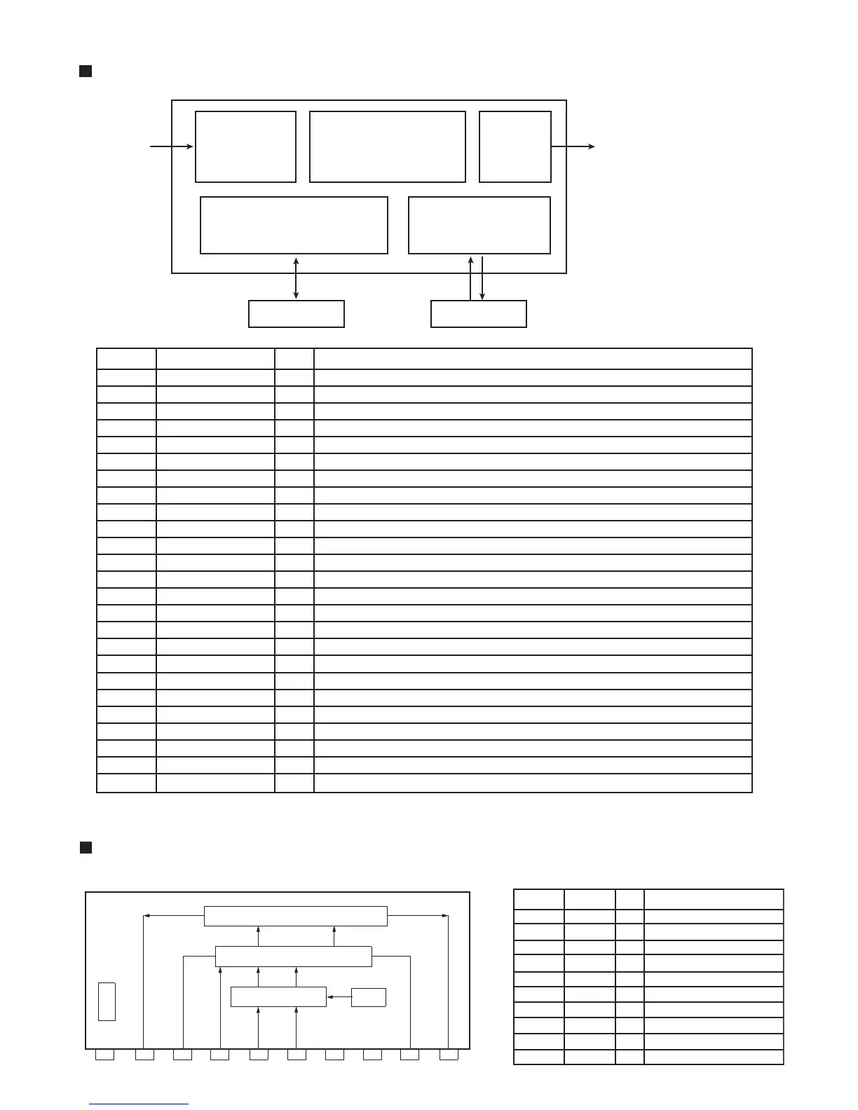
KS9274 (IC601) : CD-MP3 decoder
1.Block diagram
2.Pin function
CD-ROM Decoder MP3 Decoder
DRAM CONTROLLER
HOST MCU INTERFACE
HOST MCU
1M 4bits DRAM
DAC
INTERFACE
24-2720-22
44-63 35-39
5
6
10
14
15
20
21
22
24
25
26
27
35
36
37
38
39
44
45
46
47
50
51
52
53-62
63
CLK
RESETB
FILTER_0
FILTER_1
PLL_BYPASS
CD_DATA
CD_LRCK
CD_BCK
ACLK
BCLK
LRCK
ADAT
MDAT
MCK
MLAT
MDOUT
MINT
DDAT0
DDAT1
WEB
RASB
DDAT2
DDAT3
CASB
DA9-DA0
OEB
I
I
O
O
I
I
I
I
O
O
O
O
I
I
I
O
O
O
O
O
O
O
System clock input
System reset actibe LOW
820uF to GND940uF to GND
When "HIGH" PLL is bypassed, Tied to LOW in normal operation
Write/Read data from MCU to CD-MP3
Data strobe signal from MCU
Micom command identifier from MCU to CD-MP3
Data from CD-MP3 to MCU
Intertupt output to MCU
Data BUS
Data BUS
Wtite enable
Row address strobe
Data BUS
Data BUS
Colume address strobe
Address output
Control output to make data output to "High-Z" at DRAM
Function
Ground
Output 1
Phase compensation
Motor speed control
Input 1
Input 2
Supply voltage (Signal)
Supply voltage (Power)
Phase compensation
Output 2
I/O
-
O
-
I
I
I
-
-
-
O
DRIVER OUT
PRE DRIVER
LOGIC SWITCH
TSD
BIAS
1234
5
678910
GND
V
O1
V
Z1
V
CTL
V
IN1
V
IN2
SV
CC
PV
CC
V
Z2
V
O2
KA3082 (IC401, IC402) : DC motor driver
1.Pin layout 2.Pin function
Symbol
GND
VO1
VZ1
VCTL
VIN1
VIN2
SVCC
PVCC
VZ2
VO2
Pin No.
1
2
3
4
5
6
7
8
9
10