MIPI DSI to OpenLDI/FPD-Link/LVDS Interface Bridge Soft IP
User Guide
© 2016 Lattice Semiconductor Corp. All Lattice trademarks, registered trademarks, patents, and disclaimers are as listed at www.latticesemi.com/legal. All other brand or product names are
trademarks or registered trademarks of their respective holders. The specifications and information herein are subject to change without notice.
FPGA-IPUG-02003-1.2 15
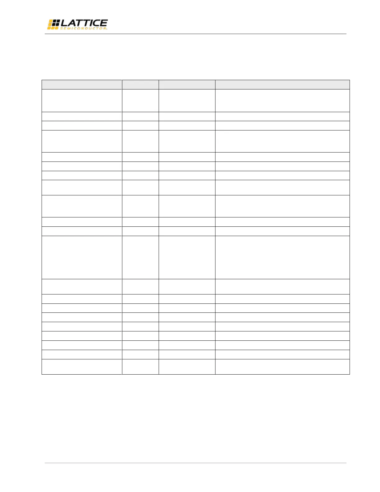
3. Parameter Settings
Table 3.1 shows the parameters used to generate MIPI DSI to OpenLDI/FPD-Link/LVDS Interface Bridge IP.
Table 3.1. MIPI DSI to OpenLDI/FPD-Link/LVDS Interface Bridge IP Parameter Settings
Number of MIPI D-PHY channels.
If 2 is selected, the following Rx settings will be applied
to both Rx channels
Number of MIPI D-PHY data lanes
Gearbox ratio of receive interface, automatically
selected based on Rx data rate (see Reset and Clocking
section on page 13)
MIPI D-PHY Implementation
Transmit interface (FPD-Link)
Derived from data type: 3 lanes for RGB666 while 4
lanes for RGB888
Gearbox ratio of transmit interface, automatically
selected based on Rx data rate (see Reset and Clocking
section on page 13)
Data rate per MIPI D-PHY lane
MIPI D-PHY clock frequency (DCK).
t
HS-SETTLE
MIPI D-PHY timing parameter is also derived
from this setting (85 ns + 6 UI).
t
HS-SETTLE
counter is implemented in byte clock domain.
The expected actual t
HS-SETTLE
is ~2 byte clock cycles
more than the computed value.
Continuous or Non-
continuous
Serializer clock frequency
Reference Clock Frequency
Reference clock frequency
Brings out miscellaneous status signals to port
Supported MIPI DSI data types
Selects between RGB666 Packed and Loosely Packed
formats