MIPI DSI to OpenLDI/FPD-Link/LVDS Interface Bridge Soft IP
User Guide
© 2016 Lattice Semiconductor Corp. All Lattice trademarks, registered trademarks, patents, and disclaimers are as listed at www.latticesemi.com/legal. All other brand or product names are
trademarks or registered trademarks of their respective holders. The specifications and information herein are subject to change without notice.
FPGA-IPUG-02003-1.2 9
lane is deserialized to byte data. The deserialization is done with 1:8 gearing or 1:16 gearing depending on Rx gear
setting (RX_GEAR). The byte data is word-aligned based on the SoT Sync sequence defined in the MIPI D-PHY
Specification version 1.1.
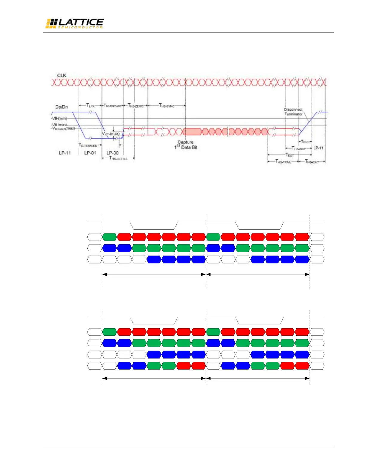
Figure 2.5. High-Speed Data Transmission
RGB data and control signals extracted from DSI packets are transmitted over FPD-Link interface such that output is
compliant to OpenLDI unbalanced format as shown in Figure 2.6 – Figure 2.8. Control signals include data enable (DE),
vertical and horizontal sync flags (VSYNC and HSYNC). Reserved bits (RES) are tied to 0.
VSYNC HSYNCDE VSYNC HSYNCDE
R0
G1
B2
R1
G2
B3
R2
G3
B4
R3
G4
B5
R4
G5
R5
B0
G0
B1
R0
G1
B2
R1
G2
B3
R2
G3
B4
R3
G4
B5
R4
G5
R5
B0
G0
B1
Current Cycle Next Cycle
clk_ch0_p_o
d0_ch0_p_o
d1_ch0_p_o
d2_ch0_p_o
Figure 2.6. FPD-Link Transmit Interface Timing Diagram (RGB666)
VSYNC HSYNCDE VSYNC HSYNCDE
R0
G1
B2
R1
G2
B3
R2
G3
B4
R3
G4
B5
R4
G5
R5
B0
G0
B1
R0
G1
B2
R1
G2
B3
R2
G3
B4
R3
G4
B5
R4
G5
R5
B0
G0
B1
Current Cycle Next Cycle
RES RESR6R7G6G7B6B7 R6R7G6G7B6B7
clk_ch0_p_o
d0_ch0_p_o
d1_ch0_p_o
d2_ch0_p_o
d3_ch0_p_o
Figure 2.7. FPD-Link Transmit Interface Timing Diagram (RGB888)