MIPI DSI to OpenLDI/FPD-Link/LVDS Interface Bridge Soft IP
User Guide
© 2016 Lattice Semiconductor Corp. All Lattice trademarks, registered trademarks, patents, and disclaimers are as listed at www.latticesemi.com/legal. All other brand or product names are
trademarks or registered trademarks of their respective holders. The specifications and information herein are subject to change without notice.
FPGA-IPUG-02003-1.2 7
Table 2.1. MIPI DSI to OpenLDI/FPD-Link/LVDS Interface Bridge IP Pin Function Description (Continued)
MIPI D-PHY channel 1 data lane 1. Available only for configurations with two Rx
channels
MIPI D-PHY channel 1 data lane 2. Available only for configurations with two Rx
channels
MIPI D-PHY channel 1 data lane 3. Available only for configurations with two Rx
channels
LVDS channel 0 clock lane
LVDS channel 0 data lane 0
LVDS channel 0 data lane 1
LVDS channel 0 data lane 2
LVDS channel 0 data lane 3. Available only for configurations with RGB888 data
type
LVDS channel 1 clock lane
LVDS channel 1 data lane 0. Available only for configurations with two Tx
channels
LVDS channel 1 data lane 1. Available only for configurations with two Tx
channels
LVDS channel 1 data lane 2. Available only for configurations with two Tx
channels
LVDS channel 1 data lane 3. Available only for configurations with two Tx
channels and RGB888 data type
Miscellaneous Status Signals
PLL lock (active high). Available only when miscellaneous status signals option
is enabled
PLL loss of lock (active high). Available only when miscellaneous status signals
option is enabled
Indicates reset sequence of DDR components is complete (active high).
Available only when miscellaneous status signals option is enabled
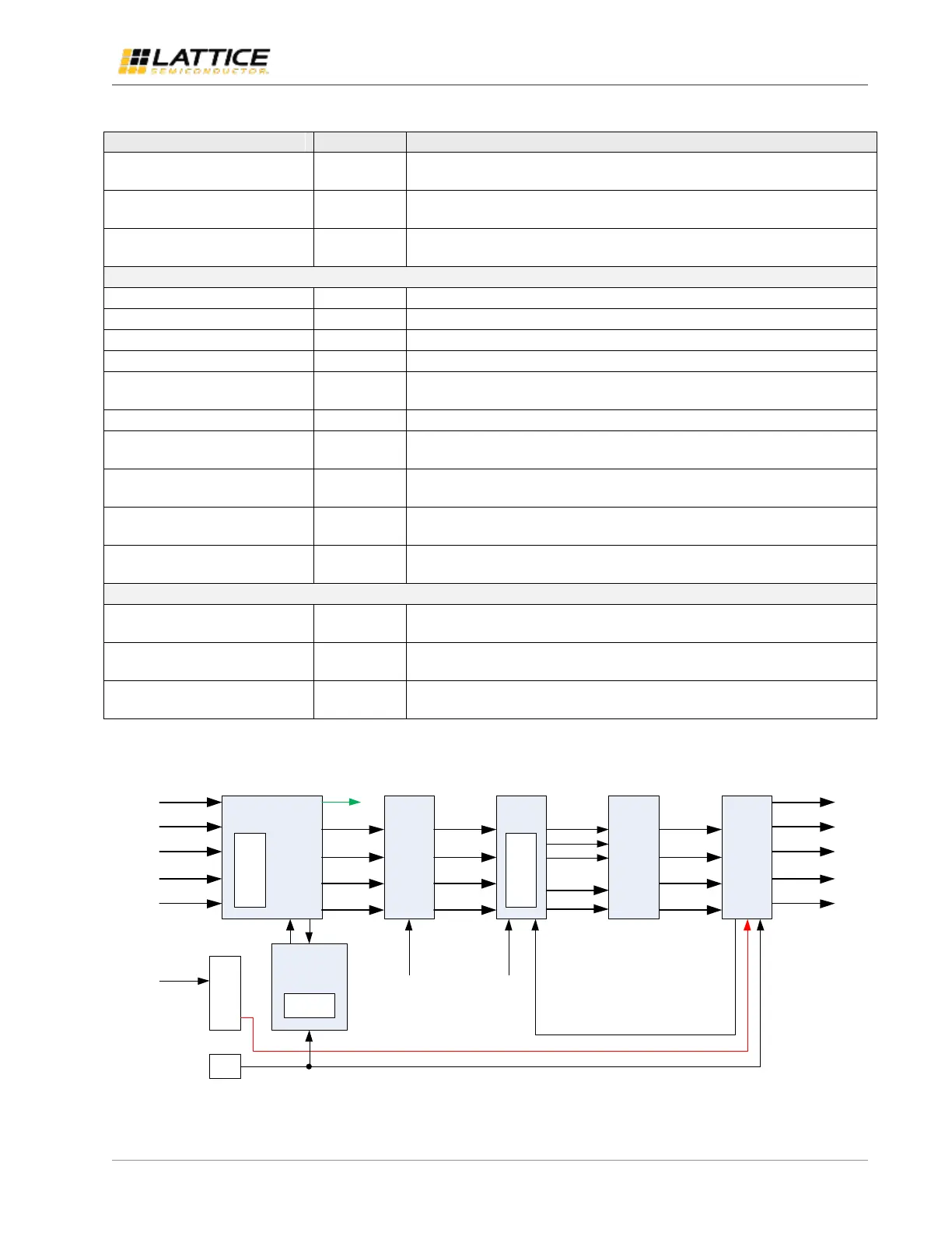
Figure 2.2 shows the single MIPI DSI to OpenLDI/FPD-Link/LVDS Interface Bridge IP (1:1) block diagram.
DPHY Common Interface
Wrapper
Hard
DPHY
RX Global
Operations
Controller
LP HS
Controller
Capture
Controller
Byte2Pixel
FIFO
PLL
clk_ch0_p_i
clk_ch0_n_i
clk_byte_fr from DPHY
clk_pixel_i
vsync_o
hsync_o
de_o
Pixel data
clk_ref_i
or
clk_byte_fr from
DPHY
d0_ch0_p_i
d0_ch0_n_i
d1_ch0_p_i
d1_ch0_n_i
d2_ch0_p_i
d2_ch0_n_i
d3_ch0_p_i
d3_ch0_n_i
Lane Distr
p_odd_o
LVDS
Wrapper
clk_ch0_p_o
clk_ch0_n_o
d0_ch0_p_o
d0_ch0_n_o
d1_ch0_p_o
d1_ch0_n_o
d2_ch0_p_o
d2_ch0_n_o
d3_ch0_p_o
d3_ch0_n_o
OSC
clk_lp_ctrl
eclk
clk_ref_i
or
clk_byte_fr from
DPHY
clk_ref_i
or
clk_byte_fr from
DPHY
Figure 2.2. Single MIPI DSI to OpenLDI/FPD-Link/LVDS Interface Bridge IP (1:1) Block Diagram