MIPI DSI to OpenLDI/FPD-Link/LVDS Interface Bridge Soft IP
User Guide
© 2016 Lattice Semiconductor Corp. All Lattice trademarks, registered trademarks, patents, and disclaimers are as listed at www.latticesemi.com/legal. All other brand or product names are
trademarks or registered trademarks of their respective holders. The specifications and information herein are subject to change without notice.
6 FPGA-IPUG-02003-1.2
2. Functional Description
The MIPI DSI to OpenLDI/FPD-Link/LVDS Interface Bridge IP serves as a bridge between a MIPI DSI host and a display
device.
2.1. Top
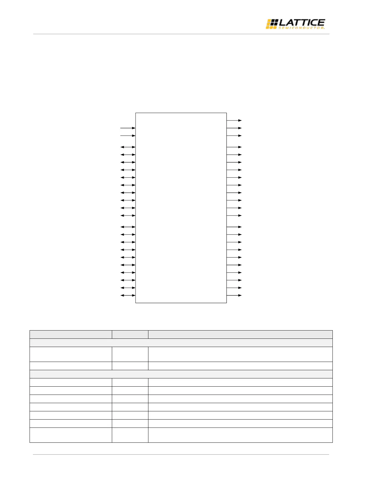
Figure 2.1 shows the MIPI DSI to OpenLDI/FPD-Link/LVDS Interface Bridge IP block diagram.
reset_n_i
clk_ref_i
clk_ch0_p_i
clk_ch0_n_i
d0_ch0_p_i
d0_ch0_n_i
d1_ch0_p_i
d1_ch0_n_i
d2_ch0_p_i
d2_ch0_n_i
d3_ch0_p_i
d3_ch0_n_i
clk_ch1_p_i
clk_ch1_n_i
d0_ch1_p_i
d0_ch1_n_i
d1_ch1_p_i
d1_ch1_n_i
d2_ch1_p_i
d2_ch1_n_i
d3_ch1_p_i
d3_ch1_n_i
clk_ch0_p_o
clk_ch0_n_o
d0_ch0_p_o
d0_ch0_n_o
d1_ch0_p_o
d1_ch0_n_o
d2_ch0_p_o
d2_ch0_n_o
d3_ch0_p_o
d3_ch0_n_o
clk_ch1_p_o
clk_ch1_n_o
d0_ch1_p_o
d0_ch1_n_o
d1_ch1_p_o
d1_ch1_n_o
d2_ch1_p_o
d2_ch1_n_o
d3_ch1_p_o
d3_ch1_n_o
lock_pll_o
pll_lol_o
ready_o
Figure 2.1. MIPI DSI to OpenLDI/FPD-Link/LVDS Interface Bridge IP Block Diagram
Table 2.1. MIPI DSI to OpenLDI/FPD-Link/LVDS Interface Bridge IP Pin Function Description
Reference clock for internal PLL. Available only when MIPI D-PHY clock is non-
continuous
Asynchronous system reset (active low)
MIPI D-PHY channel 0 clock lane
MIPI D-PHY channel 0 data lane 0
MIPI D-PHY channel 0 data lane 1
MIPI D-PHY channel 0 data lane 2
MIPI D-PHY channel 0 data lane 3
MIPI D-PHY channel 1 clock lane
MIPI D-PHY channel 1 data lane 0. Available only for configurations with two Rx
channels