– 2.4 –
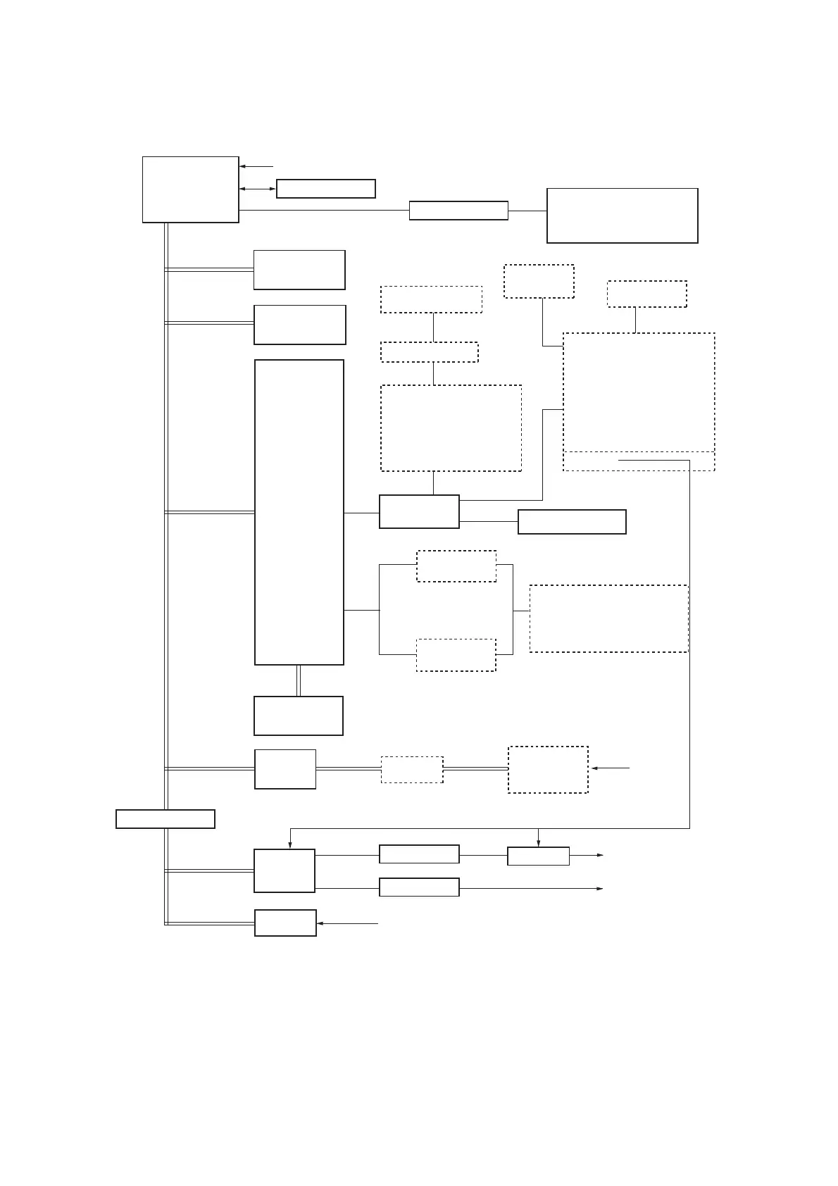
Main PCB block diagram
(SH-3 133MHz)
CPU
RTC & battery
External interruption (NMI=Power supply down, ServoG/A, PDC-CTR, 1284-CTR)
3.3/5V Buffer
Take-up PCB
Take-up switch
Take-up motor
LCD
(6 line x 2)
Keyboard PCB
Ink pack presence/absense S x
4
Ink end S x
4
Vacuum Fan x 3 (JV3-130SPII, 160SP)
Vacuum Fan x 2 (JV3-75SPII)
High-speed SRAM
(512KB x2)
X32
X32
FLASH ROM
(1MB x2)
3.3/5V Buffer
X32
X32
I/O-CTR
IO PCB
Origin S
Clamp S
Paper S
Ink cartridge presence/absence S x 4
Ink cartridge end S x 4
Ink cartridge ID S x 4
Wiper S
Pump motor x2
Wiper motor
Cover S x2
IO 2 PCB
Fan relay PCB
Fan branch PCB
Power Switch
Heater SSR x 2
Heater themistor x 2
Heater LED x 4
Heater Switch
Deodorise fan motor (inside)*
Deodorise fan motor (outside) x 2*
* (JV3-75SPII option)
Ink cartridge ID x 4
X32
HDC-CTR
HDC-CTR
Slider PCB
Cutter Solenoid
Paper Width S
Linear encoder
Head x 4
Head height S
(JV3-75SPII, 130SPII, 130SL)
S-DRAM
(32MB x4)
3.3/3.3V
Buffer
Interface PCB
1394 PCB
CPU
(SH2-28.7MHz)
IEEE1394
3.3/5V Buffer
X16
X8
Servo GA
E300237A
Motor driver
Motor driver
RERAY
1284-CTR
IEEE1284
Y motor
X motor
X2 : JV3-130SPII, 160SP
X1 : JV3-75SPII OPTION
Drying fan motor x4 (JV3-75SPII)
Drying fan motor x6 (JV3-130SPII)
Drying fan motor x7 (JV3-160SP)
 Loading...