Hardware Reference Guide SST-DN4-PCU
Hardware Register Details 31
©2009 Molex Inc.Automation & Electrical Products, Integrated Products Division
Document Edition: 1.0, Document #: 715-0101, Template Edition: 1.1, Template #: QMS-06-045
Use, duplication or disclosure of this document or any of the information contained herein is subject to the restrictions on page ii of this document.
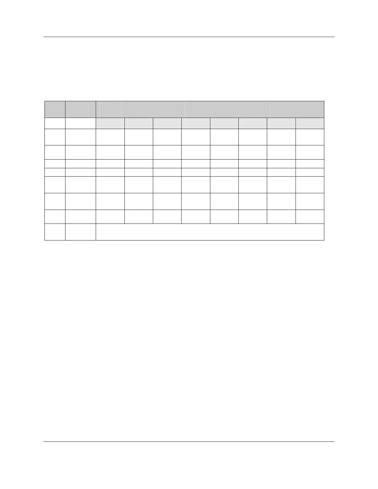
Table 6: Host Register Layout
The following “offsets” are offsets from the base address. An “X” means that the bit is reserved
(writing to it will result in undefined behavior).
Offset Register Bit Name
Name
7 6 5 4 3 2 1 0
00h Control CardRun
(r/w)
MemEn
(r/w)
IntEn
(r/w)
WdTout
(read)
0
HostIrq0
(r/w)
0
CardIrq0
(r/w)
01h
(rd)
AddrMatch 1 X X X X X X 0
02h BankAddress 0 0 BA17 BA16 BA15 BA14 BA13 BA12
03h BankSize 0 0 WS17 WS16 WS15 WS14 WS13 WS12
04h HostIrq
(r/w)
Platform X X X X X X X
05(rd) LedReg
(read)
X X PwrRed PwrGrn HealthRed HealthGrn CommRed CommGrn
06h Debug
(r/w)
X X X X X X X X
07
(rd)
HDR
(FamilyID)
HostDataReg (written by CPU)
DN4 = 40h