Hardware Reference Guide SST-DN4-PCU
Hardware Register Details 33
©2009 Molex Inc.Automation & Electrical Products, Integrated Products Division
Document Edition: 1.0, Document #: 715-0101, Template Edition: 1.1, Template #: QMS-06-045
Use, duplication or disclosure of this document or any of the information contained herein is subject to the restrictions on page ii of this document.
3.4.3 AddrMatch Register
This register is reserved.
3.4.4 Bank Address Register
This register is used to switch banks of shared memory into host memory space.
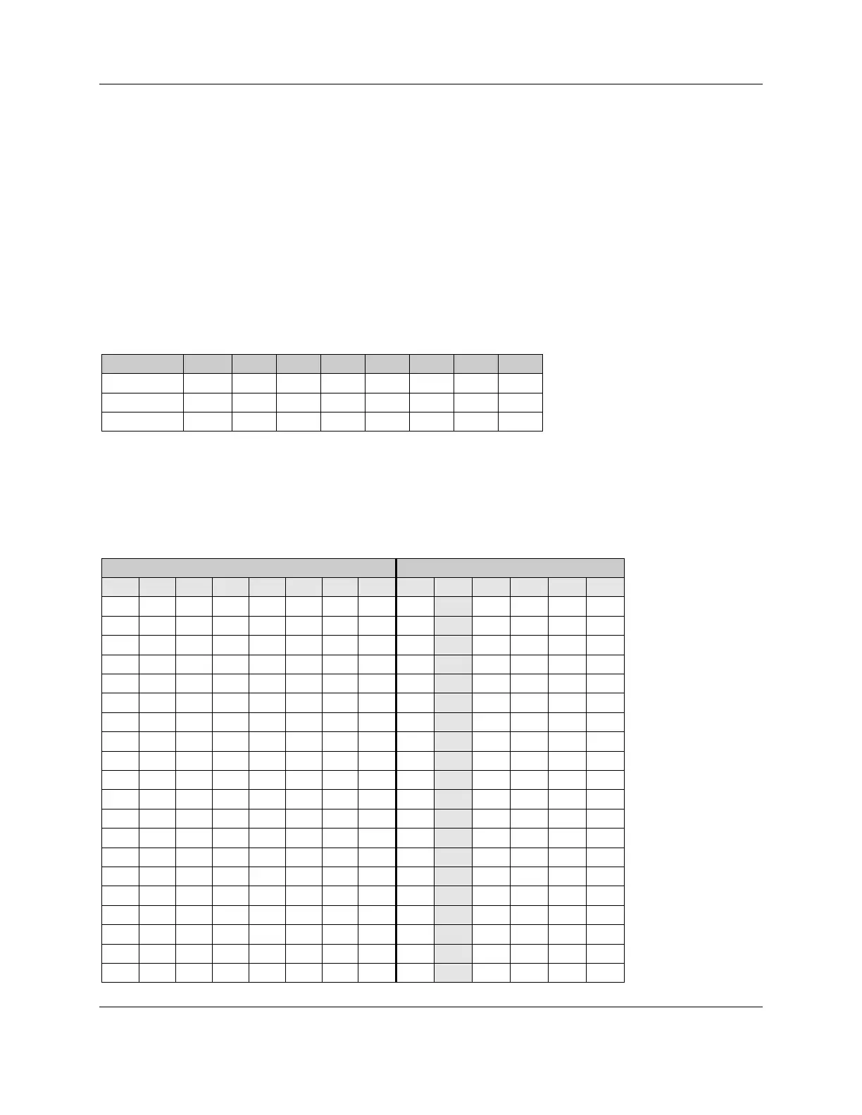
Table 9: Bank Address Register Settings
Bit 7 6 5 4 3 2 1 0
Name BA19 BA18 BA17 BA16 BA15 BA14 BA13 BA12
Read/Write R R R/W R/W R/W R/W R/W R
Reset 0 0 0 0 0 0 0 0
Table 10: Bank Address Register Values
In this table, the default window size is highlighted, and a value of “x” indicates “don’t care”.
Bit and Value Window Size and Bank Number
BA19 BA18 BA17 BA16 BA15 BA14 BA13 BA12 8k 16k 32k 64k 128k 256k
x x 0 0 0 0 0 x 0 0 0 0 0 0
x x 0 0 0 0 1 x 1 0 0 0 0 0
x x 0 0 0 1 0 x 2 1 0 0 0 0
x x 0 0 0 1 1 x 3 1 0 0 0 0
x x 0 0 1 0 0 x 4 2 1 0 0 0
x x 0 0 1 0 1 x 5 2 1 0 0 0
x x 0 0 1 1 0 x 6 3 1 0 0 0
x x 0 0 1 1 1 x 7 3 1 0 0 0
x x 0 1 0 0 0 x 8 4 2 1 0 0
x x 0 1 0 0 1 x 9 4 2 1 0 0
x x 0 1 0 1 0 x 10 5 2 1 0 0
x x 0 1 0 1 1 x 11 5 2 1 0 0
x x 0 1 1 0 0 x 12 6 3 1 0 0
x x 0 1 1 0 1 x 13 6 3 1 0 0
x x 0 1 1 1 0 x 14 7 3 1 0 0
x x 0 1 1 1 1 x 15 7 3 1 0 0
x x 1 0 0 0 0 x 16 8 4 2 1 0
x x 1 0 0 0 1 x 17 8 4 2 1 0
x x 1 0 0 1 0 x 18 9 4 2 1 0
x x 1 0 0 1 1 x 19 9 4 2 1 0