Hardware Reference Guide SST-DN4-PCU
Hardware Register Details 35
©2009 Molex Inc.Automation & Electrical Products, Integrated Products Division
Document Edition: 1.0, Document #: 715-0101, Template Edition: 1.1, Template #: QMS-06-045
Use, duplication or disclosure of this document or any of the information contained herein is subject to the restrictions on page ii of this document.
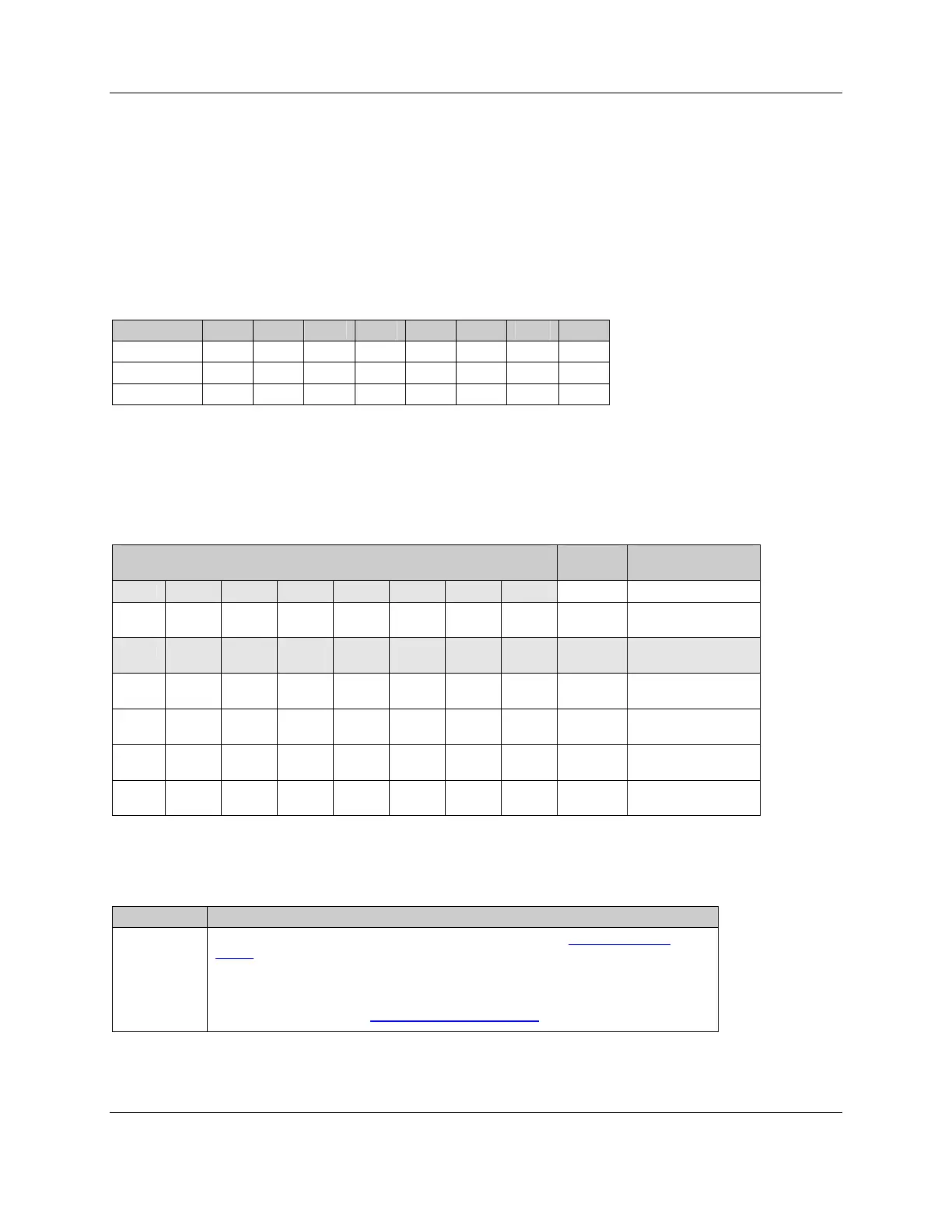
3.4.5 BankSize Register
This register controls the window size by masking off bits BA19-BA12 in the Bank Address
register. Table 13, BankSize Register Values, maps the WS values required for each valid
window size.
Table 12: BankSize Register Settings
Bit 7 6 5 4 3 2 1 0
Name WS19 WS18 WS17 WS16 WS15 WS14 WS13 WS12
Read/Write R R R/W R/W R/W R/W R/W R
Reset 0 0 0 0 0 0 1 1
Table 13: BankSize Register Values
In this table, the default window values are highlighted.
Bit and Value Window
Size
Description
WS19 WS18 WS17 WS16 WS15 WS14 WS13 WS12
0 0 0 0 0 0 0 1 8K BA19-BA13 used,
BA12 ignored
0 0 0 0 0 0 1 1 16K BA19-BA14 used,
BA13-BA12 ignored
0 0 0 0 0 1 1 1 32K BA19-BA15 used,
BA14-BA12 ignored
0 0 0 0 1 1 1 1 64K BA19-BA16 used,
BA15-BA12 ignored
0 0 0 1 1 1 1 1 128K BA19-BA17 used,
BA16-BA12 ignored
0 0 1 1 1 1 1 1 256K BA19-BA18 used,
BA17-BA12 ignored
Table 14: BankSize Register Bit Descriptions
Bit Name Description
WS19-WS12 WS19-WS12 represent the window size, according to Table 15: BankSize Register
Values.
• Writing any value other than those above has no effect
The size of the memory window affects the number of banks required to access all
memory. Refer to Table 12:
Bank Address Register Values, for more information.