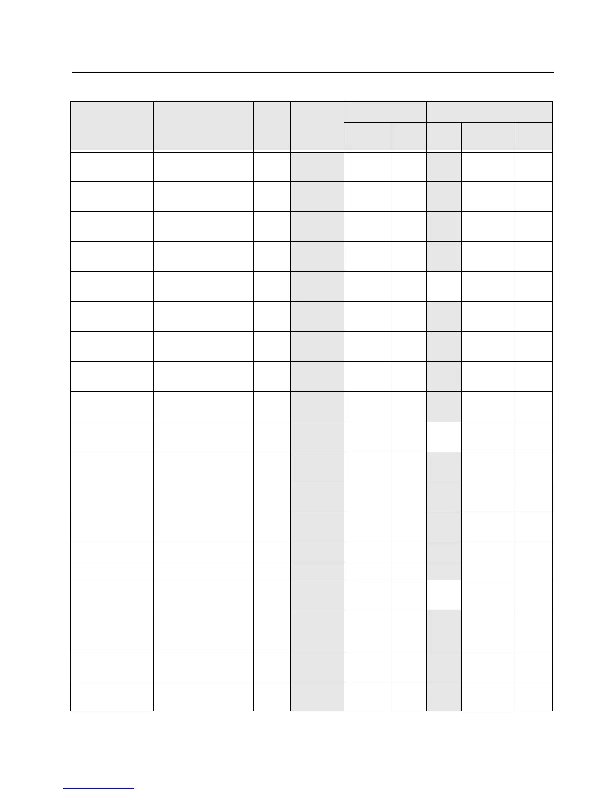
Troubleshooting Tables: List of Board and IC Signals 7-11
spi_arm_miso ARM SPI Data into
OMAP
U18
Input Pull-
down
Input Pull-
down
spi_dsp_clk DSP SPI Clock from
OMAP
N14
I/O Pull-
down
Input None
spi_dsp_mosi DSP SPI Data from
OMAP
P14
Output Pull-
down
Input Pull-
down
spi_dsp_miso DSP SPI Data into
OMAP
AA17
Input Pull-
down
Input Pull-
down
gps_uart_tx UART Data from
OMAP to GPS IC
M18
Output None 0 Output Pull-
down
gps_uart_rx UART Data from GPS
IC to OMAP
R9
Input Pullup Input Pull-
down
16.8_mhz_clk Timer Reference
Clock Input
N18
Input None Input Pull-
down
trident_ssi[0] Transmit SSI Clock
from RF Board
Y6
Input Pull-
down
Input Pull-
down
trident_ssi[1] Transmit SSI Frame
Sync from RF Board
W7
Input Pull-
down
Input Pull-
down
trident_ssi[2] Transmit SSI Data
from OMAP
AA5
Output Pull-
down
0 Output Pull-
down
abacus_ssi[0] Receive SSI Clock
from RF Board
V7
I/O Pull-
down
Input None
abacus_ssi[1] Receive SSI Frame
Sync from RF Board
W6
I/O Pull-
down
Input None
abacus_ssi[2] Receive SSI Data
from RF Board
P10
Input Pull-
down
Input Pull-
down
scl I2C Clock T18
I/O None Input None
sda I2C Data V20
I/O None Input None
rtck JTAG Clock from
Controller
Y17
I/O None U Unknown None
tck JTAG Clock from
JTAG box to
Controller
W18
Input None Input Pull-
down
ntrst JTAG Reset from
JTAG box
Y18
Input None Input
omap_tms JTAG Test Mode
Select from JTAG box
V17
Input Input Pull-
down
Table 7-7. Overall GPIO pin functions (Continued)
Signal Name Description
Pin or
Ball #
Active State
SW Initialized HW Reset
Direction
*
PU State Direction
*
PU
or
PD
 Loading...