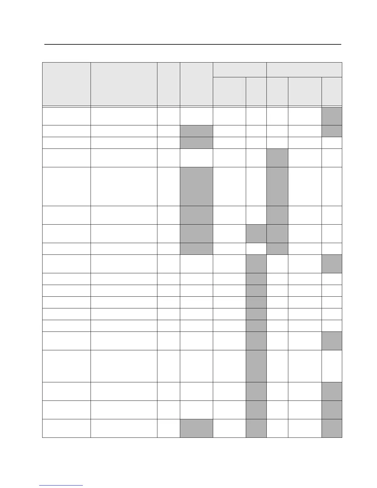
Troubleshooting Tables: List of Board and IC Signals 7-17
MORTABLE Specifies Mobile or
Portable hardware
W13 0=Portabl
e
Input None 0 Output
GCAI_GPIO3 GCAI pin 9, GPIO3 AA15 Input None 0 Output
GCAI_GPIO4 GCAI pin 12, GPIO4 R14 Input None Input PD
BLUETOOTH_P
TT
PTT signal from
Bluetooth AVR
Y5 0=Pressed Input PU
Input PD
F2_TIMER_INP
UT_CAPTURE
Receives one of three
timing signals mux’ed
through CPLD - Abacus
Sync, DMCS, Ramp
DAC Trigger.
P20
Input PD Input PD
BT_AVR_STATU
S
AVR status read by
OMAP
P18 Input PU Input PD
ACC_SPKR_UN
MUTE
BT_Audio_Accessory_U
nmute signal
K15
Output Input PU
BT_SPARE_1.8 Bluetooth_Spare_GPIO K14
I/0 PD Input PD
ENC_WAKEUP MACE encryption
wakeup
A6 1 Output
1 Output
ENC_RESET MACE encryption reset B6 0 I/O PU 1 I/O PU
5V_PWM_EN Forces SW5 to PWM P14 1 Output
PU 0 Output PU
GCAI_GPIO2 GCAI pin 5, GPIO2 C13 Input
None Input None
GCAI_GPIO1 GCAI pin 4, GPIO1 C11 Input
None Input None
GCAI_GPIO0 GCAI pin 1, GPIO0 M7 Input
None Input None
GCAI_VBUS_I_
LIMIT
Current limit select for
GCAI VBUS
C6 1=500mA Output
0 Output
F2_PARAMP_M
ON
Factory use to test F2
transmit timing. Allows
TX/RX signal to appear
on GCAI GPIO3.
C5 1=Factory
Tes t
Output PU 0 Output PU
TOP_DISP_DAT
A_CTRL
Select for data or control
on top display
P12 1=data Output 0 Output
TOP_DISPLAY_
RESET
Reset for color front
display
M12 0 Output 1 Output
Unused and Unwired
OMAP Pin
N13 Output 0 Output
Table 7-12. Overall GPIO pin functions across multiple boards (Continued)
Signal Name Description
Pin
or
Ball #
Active
State
SW Initialized HW Reset
Direction
*
PU State Direction
*
PU
or
PD

 Loading...