N720 OpenLinux
Hardware User Guide
Copyright © Neoway Technology Co., Ltd
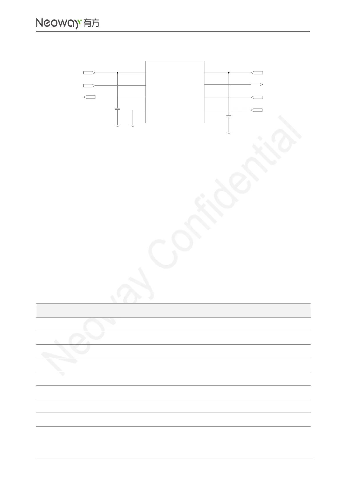
Figure 3-20 Recommended level shifting circuit 3
VL
IO_VL1
GND
IO_VL2
VCC
IO_VCC1
IO_VCC2
EN
NLSX4373
VDD_1P8
UART_TXD
UART_RXD
VDD_1P8
VCC_IO
MCU_RXD
MCU_TXD
0.1μF
0.1μF
C1
C2
U1
Schematic Design Recommendations
NLSX4373 is a dual-supply level shifter, the rate of which can be up to 20 Mb/s.
VL is the reference voltage of IO_VL1 and IO_VL2, ranging from 1.5V to 5.5V.
VCC is the reference voltage of IO_VCC1 and IO_VCC2, ranging from 1.5V to 5.5V.
EN is the enable pin, which works at a voltage of greater than VL-0.2V. In the above circuit, the
EN pin is connected to VDD_1P8 and the level shifter is always working.
PCB Design Guidelines
Do not cross other traces if possible. If crossing is inevitable, route the UART traces
perpendicular to other traces.
Keep traces far away from areas that might introduce ESD.
Surround the traces with the ground plane if possible.
3.3.5 SDC
Control of SD external power