N720 Hardware User Guide
Copyright © Neoway Technology Co., Ltd 38
3.2 GNSS RF Design and PCB Layout
3.2.1 GNSS Impedance
The 92nd pin is the GNSS interface of the module, which also requires a 50 Ω. The PCB layout for GNSS
is similar to that for GPRS. For details, refer to the previous section. Figure 3-5 shows the internal
structure of the GNSS RF.
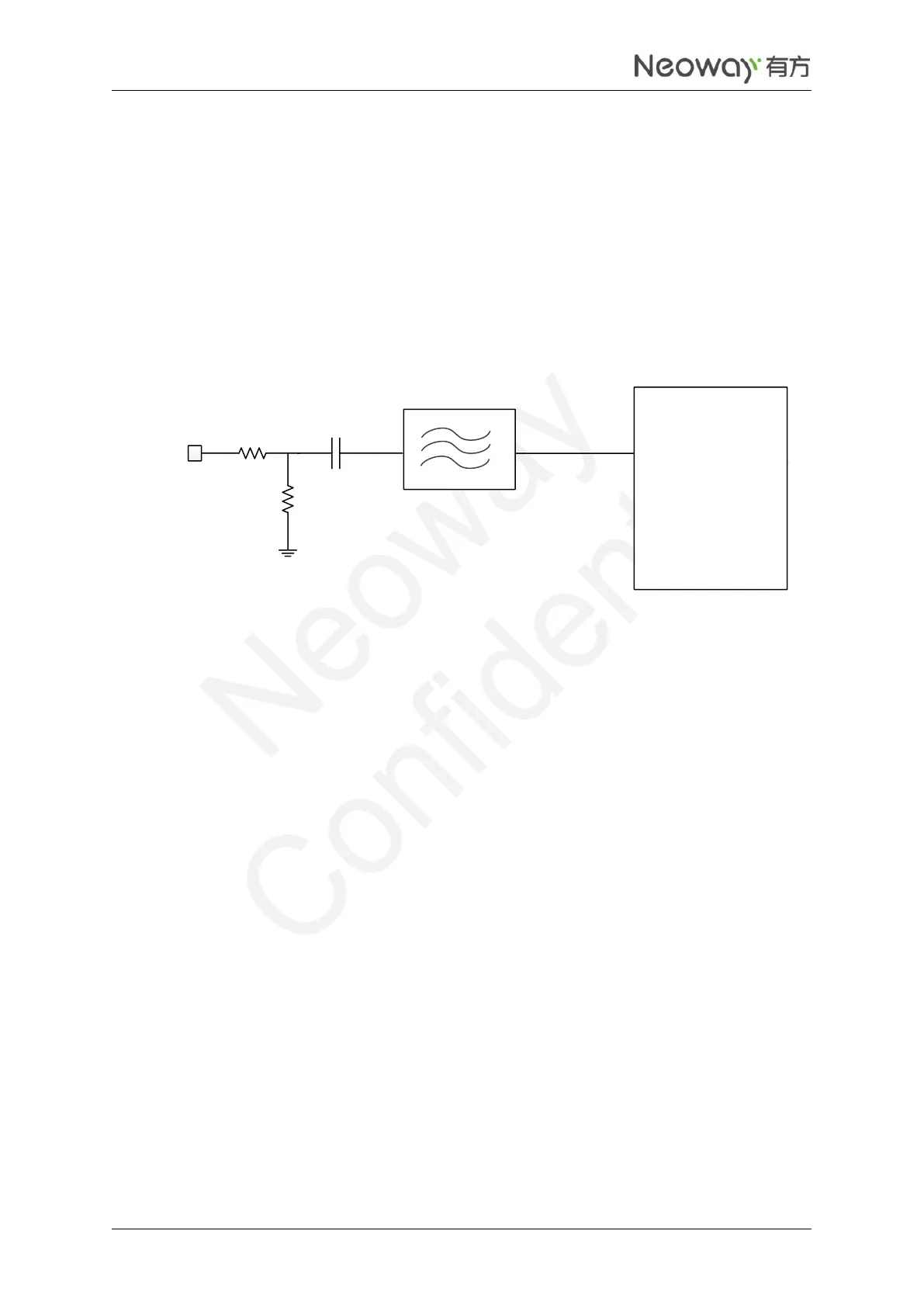
Figure 3-5 GNSS RF structure
WTR GPS Interface
SAW
ANT_GNSS
In addition to the basic rules, the GNSS routing has higher requirements because the air wireless GNSS
signal has lower strength, which results in weaker electrical signal after the antenna receives. Weaker
signals are more susceptible to interference. Therefore, active antenna are commonly used for GNSS. The
active GNSS antenna amplifies the weak signals received to stronger signals through the low-noise
amplifier (LNA) and then transmits the signals through the feeder.
If using a passive antenna, add LNA near the feeder because the module does not embed one internally.
If the antenna and layout are not designed reasonably, the GNSS will be insensitive, resulting in long time
on positioning or inaccurate position.
Keep the GPRS and GNSS far away from each other in layout and antenna layout design.
3.2.2 Active GNSS Antenna Design
Ceramic GNSS chip antenna is mainly used. In general, using the active ceramic antenna is recommended.
After the antenna receives GNSS satellite signals, the LNA amplifies them first and then they are
transmitted to the 92nd pin (GNSS_ANT) through the feeder and PCB traces. 50 Ω impedance is required
for both the feeder and PCB traces and the traces should be as short as possible. The power supply of the
active antenna is fed by the 100 nH inductance through the signal traces.