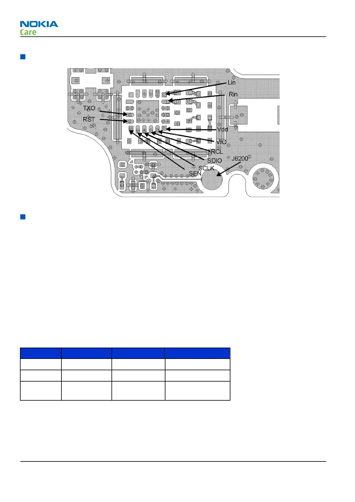
FMTx 2.1 PWB traces
Figure 54 FMTx 2.1 layout
Specific digital and power supply test points
Using access to signals figure as a reference it can be seen that supplies to the Si4713 device VIO (pin 10) and
VDD (pin 11) can be accessed easily. The FMTx 2.1 solution utilises a QFN package. This type of package lends
itself well to analysis of signals on the various pins of the device.
VIO & VDD
VIO should be in the range 1.5 to 3.6 Volts.
VDD should be in the range 2.7 to 5.5 Volts.
_RST
Also, the _RST signal to the device can be monitored. This is an active low signal and should only be asserted
during power up. The _RST signal is driven by the PURX line.
The state of pins 19 & 18 (GPO1 and GP02 respectively) on the rising edge of the _RST pin determines what
interface is selected when the device powers up.
Table 6 Bus mode selection truth table
Bus Name Bus Mode GPO1 GPO2/IRQ
I2C 2-Wire High Low
SPI SPI High Low (must drive)
CBus 3-Wire Low (must
drive)
Low
It’s possible that if GP01 and/or GPO2 are not at the correct state when the Si4713 device has power applied
then the wrong bus mode could be selected and the handset would be unable to communicate with the
device. For RM-484, the bus mode should be I2C.
RM-484; RM-485; RM-486
FMTx 2.1 Troubleshooting
Page 7 –6 COMPANY CONFIDENTIAL Issue 1
Copyright © 2009 Nokia. All rights reserved.