Hardware description
4.3.4 nRF5340 power source
The nRF5340 DK has a power source switch (SW9) for selecting between VDD (default), Li-Po, and USB
power supplies for the nRF5340 SoC.
VDD_nRF_SENSE
C65
100nF
V5V
3
2
1
A
84
V- V+
U9A
TS27L2IPT
VSENSE_SW_OUT
R70
10M
Q9
RV2C010UNT2L
R69
1M0
VSUPPLY
Q7
FCX690BTA
SB39
VSUPPLY_EN
TP33
TP34
VIO_REF
R77
10k
VIN
A2
VOUT
A1
CTRL
B2
GND
B1
U14
TCK106AG
VIN
A2
VOUT
A1
CTRL
B2
GND
B1
U12
TCK106AG
R12
47k
R8
1M0
C22
10nF
Q3
RV2C010UNT2L
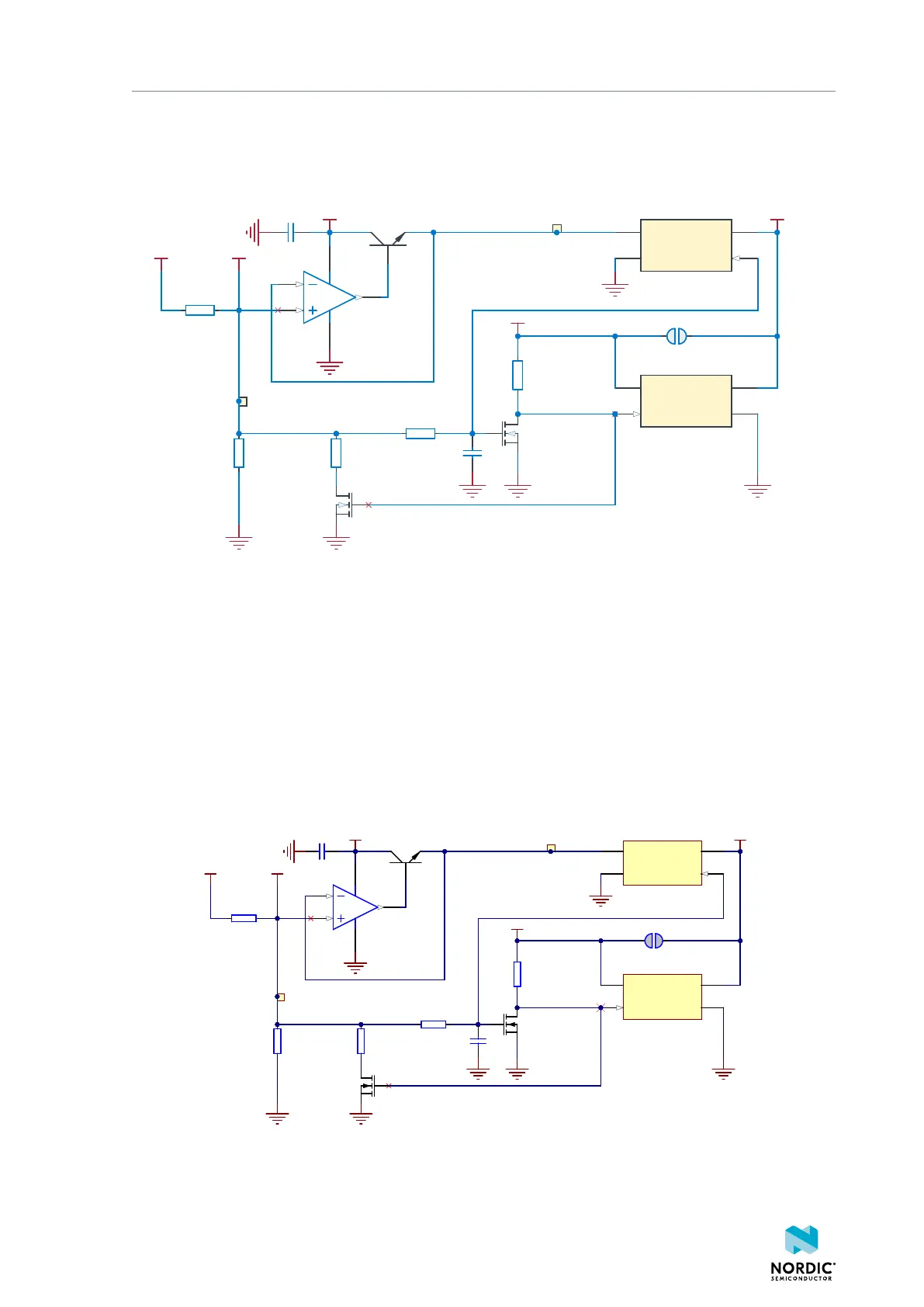
Figure 12: nRF5340 DK power source switch
The nRF5340 SoC has a high voltage buck regulator that can support up to 5 V input. In the VDD position,
the SoC is powered from the onboard buck regulator, coin cell battery, or external supply (P21). In the Li-
Po position, the high voltage regulator of the SoC is supplied directly from the Li-Poly battery connectors
(J6 or P27). In the USB position, the USB high voltage regulator is powered by thenRF5340 USB connector
(J3).
When the high voltage regulator is used, the VDD_nRF voltage can be set by SoC firmware. To make sure
the rest of the DK has the same voltage level, the VDD of the DK is sourced by a regulator following the
VDD_nRF voltage when the high voltage regulator is used.
VDD_nRF_SENSE
C65
100nF
V5V
3
2
1
A
84
V- V+
U9A
TS27L2IPT
VSENSE_SW_OUT
R70
10M
Q9
RV2C010UNT2L
R69
1M0
VSUPPLY
Q7
FCX690BTA
SB39
VSUPPLY_EN
TP33
TP34
VIO_REF
R77
10k
VIN
A2
VOUT
A1
CTRL
B2
GND
B1
U14
TCK106AG
VIN
A2
VOUT
A1
CTRL
B2
GND
B1
U12
TCK106AG
R12
47k
R8
1M0
C22
10nF
Q3
RV2C010UNT2L
Figure 13: VDD_nRF voltage follower and switch
4406_638
17
 Loading...