Hardware description
CAUTION: To avoid overloading the power supply and damaging the DK, use VDD and keep the
supply below 100 mA. Do not use a Li-Poly source.
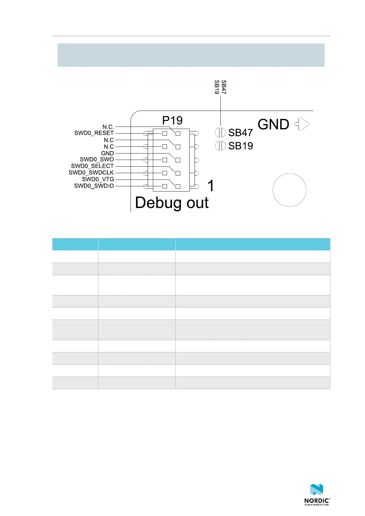
The following section includes an illustration of the P19 connector pinout with a description table.
Figure 29: Debug output connector P19
Pin number Signal Description
1 SWD0_VTG Optional voltage supply to the external target
2 SWD0_SWDIO SWD Data Input/Output
3 SWD0_SELECT Debug out select signal, connect to ground on external
board
4 SWD0_SWDCLK Serial Wire Clock line
5 GND Ground
6 SWD0_SW0 The Serial Wire Output (SWO) line is not used for
programming and debugging over SWD
7 N.C. Not used
8 N.C. Not used
9 N.C. Not used
10 SWD0_RESET Reset line
Table 8: Connector P19 pinout for programming external targets
4.10.2 Programming a board with custom connections
For boards with custom pin connections for programming and debugging, use debug output on connector
P20.
Connect the boards as shown in the following figure.
4406_638
29
 Loading...