Hardware description
To make sure that the nRF5340 SoC is not powered when the nRF power switch (SW8) is OFF, two load
switches are used, one for the high voltage regulator (U15) and one for the USB supply (U20). These
switches are controlled by VDD.
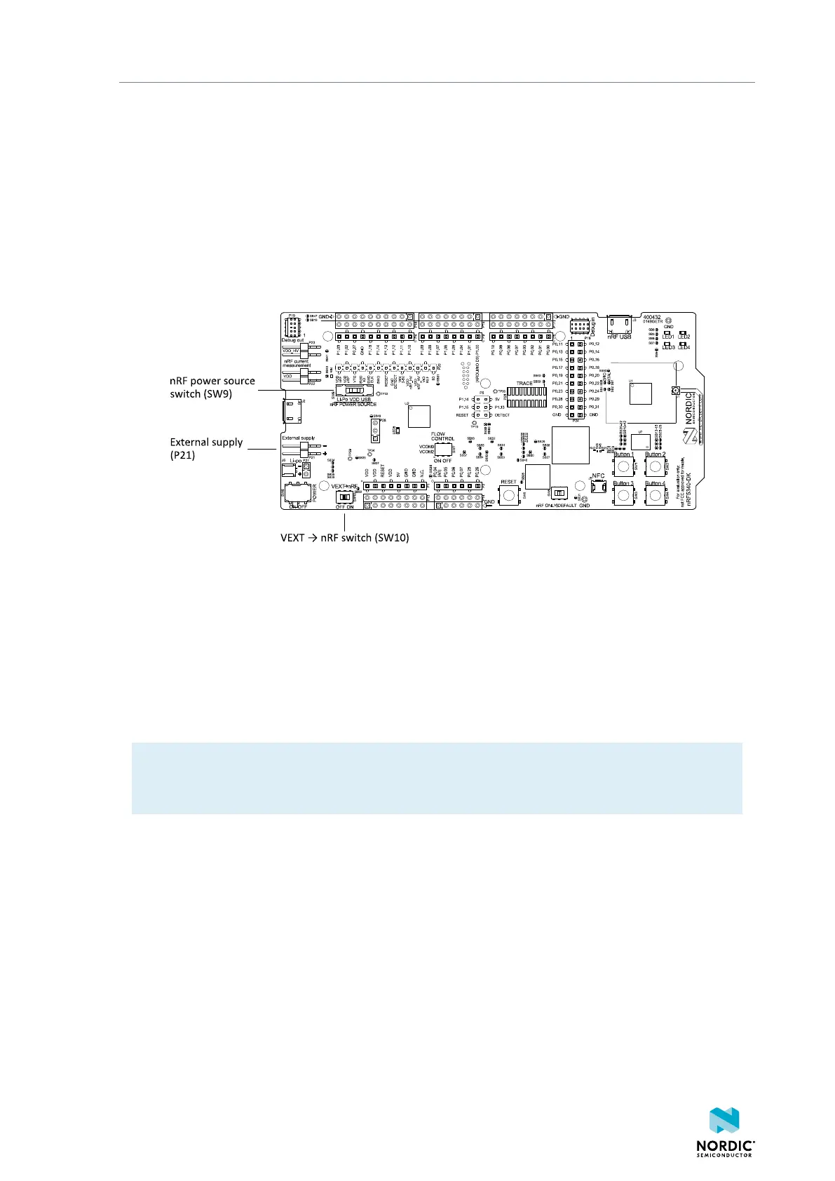
4.3.5 nRF5340 SoC direct supply
It is possible to power the application SoC directly from a source without powering the rest of the DK from
that source.
This is done by connecting the external source to the external supply connector (P21) and sliding the
VEXT->nRF switch (SW10) to the ON position. The nRF power source switch (SW9) must be in the VDD
position. The allowed voltage range is from 1.7 V to 3.6 V.
Figure 14: VEXT->nRF switch (SW10)
Since only the nRF5340 SoC is supplied from this source, it is recommended that the VDD domain is
supplied from a different source to ensure the pins of the SoC are not connected to unpowered devices.
To avoid voltage differences on the DK, the external supply is also connected to the input of the voltage
follower when the VEXT->nRF switch (SW10) is in the ON position. The voltage follower circuit requires 5 V
supplied to the DK, see 5 V power sources on page 13.
The voltage follower can be disconnected from the External supply by cutting SB58. To prevent leakage
due to voltage differences, the DK should be set in the nRF only mode, see nRF only mode on page 19.
Note: To reduce trace length and parasitic components, the external memory is connected to the
SoC directly instead of using analog switches. It is recommended to cut solder bridges to avoid
leakage, see External memory on page 21.
4.4 Modes of operation
The following sections describe signal switches and the various modes of operation of the nRF5340 DK.
4.4.1 USB detect
To detect when USB for the interface MCU is connected, there is a circuit sensing the VBUS of USB
connector J2.
When the USB cable is connected, the VDD is propagated to the USB_DETECT signal.
4406_638
18
 Loading...