Hardware description
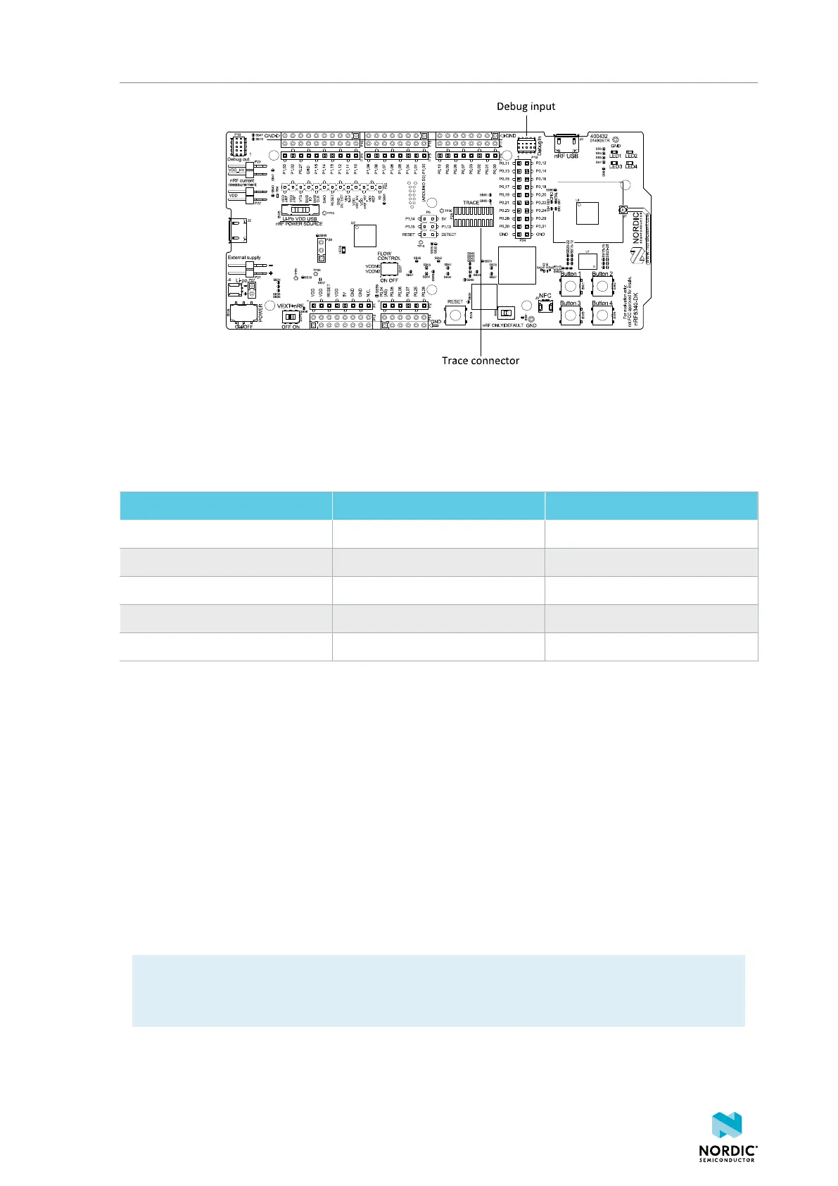
Figure 26: Debug input and trace connectors
For trace, a footprint for a 20-pin connector is available (P25). If trace functionality is required, it is
possible to mount a 2x10 pin 1.27 mm pitch surface-mount pin header. To use trace, you must disable flow
control on UART_0, by switching Flow Control (SW7) for serial port 0 to off.
GPIO Trace Default use
P0.12 TRACECLK
P0.11 TRACEDATA[0] UART_0 RTS
P0.10 TRACEDATA[1] UART_0 CTS
P0.09 TRACEDATA[2] BUTTON 4
P0.08 TRACEDATA[3] BUTTON 3
Table 7: Default and Trace GPIOs
By default, the reference voltage for the debug input and trace is connected to VDD_nRF'. This can be
connected to the VDD by cutting SB60 and soldering SB59.
4.10 Debug out for programming external boards
The nRF5340 DK supports programming and debugging external boards with an nRF51, nRF52, and nRF53
Series SoC, or the nRF91 Series System in Package (SiP).
The interface MCU on the nRF5340 DK runs SEGGER J-Link OB interface firmware. It is used to program
and debug the application firmware of the nRF5340 SoC, by default.
To program/debug an external board instead, connect to the Debug out connector (P19) using a 10-pin
cable or use P20 for custom connection.
Note: It is recommended to power the external board separately from the DK. The voltage on the
external board must match that of the DK. When the DK is powered through the USB connector,
the voltage is 3V.
4406_638
27
 Loading...