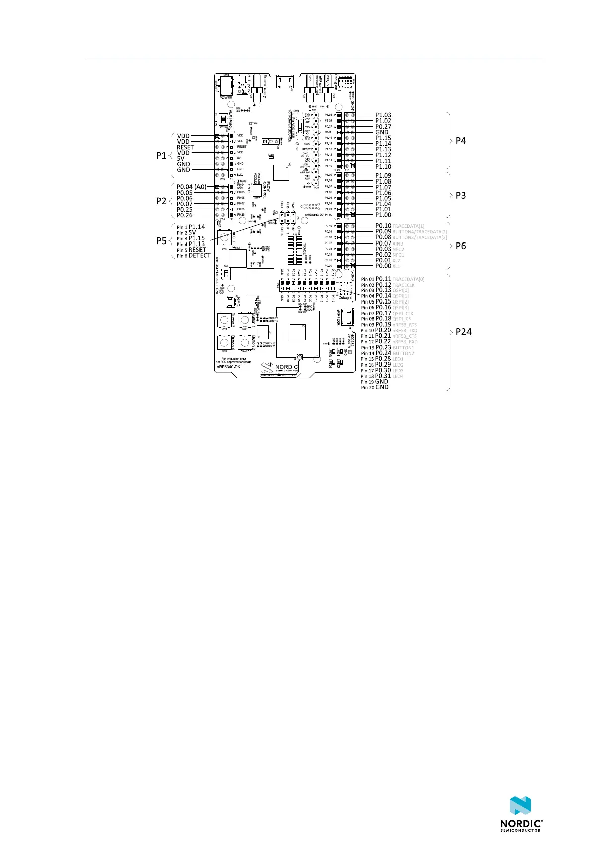
Hardware description
Figure 20: nRF5340 DK connectors
Some of the signals are also available on connectors P7, P8, P9, P10, P11, and P12, located on the back
side of the DK. By mounting pin lists on the connector footprints, the nRF5340 DK can be used as a shield
for 3.3 V Arduino motherboards or other boards that follow the Arduino standard.
For easy access to GPIO, power, and ground, the signals can also be found on the through-hole connectors
P13–P17.
The following are default pin settings:
• P0.00 and P0.01 are used for the 32.768 kHz crystal and are not available on the connectors. See
32.768 kHz crystal on page 26 for more information.
• P0.19, P0.20, P0.21, and P0.22 are used by the UART connected to the interface MCU. See
Virtual serial ports on page 8 for more information.
• P0.02 and P0.03 are by default used by signals NFC1 and NFC2. See NFC antenna interface on page
32 for more information.
• P0.08–P0.09 and P0.23–P0.24 are by default connected to the buttons and P0.28–P0.31 are
connected to the LEDs. See Buttons and LEDs on page 24 for more information.
• P0.13–P0.18 are by default connected to the external memory. For more information, see External
memory on page 21.
When the nRF5340 DK is used as a shield together with an Arduino standard motherboard, the Arduino
signals are routed as shown in the following figure.
4406_638
23
 Loading...