USB and PCIe
PRELIMINARY INFORMATION
Jetson Orin NX Series and Jetson Orin Nano Series DG-10931-001_v1.1 | 39
Routing to M.2 (NVMe) connector/card:
Insertion loss / length (delay)
Gen 4.0: -1.51 dB/in @ 8Ghz
Gen 3.0: -0.86 dB/in @ 4GHz
Length to delay calculations assumes 6.4
ps/mm (average of stripline and
microstrip).
The 2
nd
Orin Module loss assumption is:
Gen 4.0: -8 dB @ 8GHz
Gen 3.0: -6.5 dB @4GHz
The PCIe/M.2 connector/card loss
assumption is:
Gen 4.0: -9.5 dB @ 8GHz
Gen 3.0: -8.2 dB @4GHz
Gen 3.0 max trace:
Direct to device:
Insertion loss / length (delay)
Routing to 2
nd
Orin Module
Insertion loss / length (delay)
Routing to PCIe/M.2 connector/module:
Insertion loss / length (delay)
-15.8 / 467 (2987)
-10.5 / 310 (1985)
-7.6 / 224 (1437)
Max PCB via delay from the
Device/Connector
Max distance from Device ball or
Connector pin to first PCB via.
PCB within pair (intra-pair) skew
Do trace length (delay) matching before
hitting discontinuities.
Within pair (intra-pair) matching between
subsequent discontinuities
Differential pair uncoupled delay
Place GND vias as symmetrically as possible to data pair vias. GND via distance
should be placed less than 1x the diff pair via pitch
Use micro via or back drilled via - no via
stub allowed.
20%, 0402 X5R or better. Only required
for TX pair when routed to connector.
Place close to TX side.
Voiding the plane directly under the pad
~0.1mm larger than the pad size is
required.
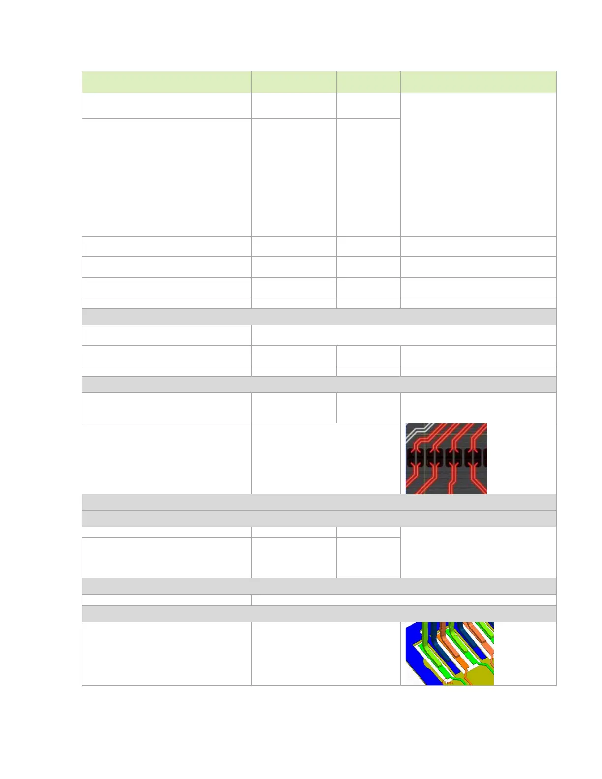
Serpentine (See USB 3.2 Guidelines)
S1 must be taken care in order to
consider Xtalk to adjacent pair. (
Dimension
Min A Spacing
Min B, C Length
Min Jog Width
Remove unwanted GND fill that is either floating or act like antenna
Void all layers of golden finger area
under the pad ~0.15mm larger than the
pad size is recommended.
 Loading...


